Optimization of LGAD Detectors: SIMDET 2016 Research Overview
Research conducted at IMB-CNM in collaboration with RD50 (CERN) focused on optimizing LGAD detectors through TCAD simulations. The project delved into simulation procedures, basic detector technologies, process technology, radiation hardness enhancement, HGTD and CT-PPS simulation, and conclusions drawn from the study. IMB-CNM, a Spanish research institution, is dedicated to nano and microelectronics with advanced clean room facilities and a focus on micro and nano fabrication technologies. The research aimed at improving radiation detector performance for applications in high-energy physics, dosimetry, medical imaging, nuclear physics, and security sectors.
Download Presentation

Please find below an Image/Link to download the presentation.
The content on the website is provided AS IS for your information and personal use only. It may not be sold, licensed, or shared on other websites without obtaining consent from the author.If you encounter any issues during the download, it is possible that the publisher has removed the file from their server.
You are allowed to download the files provided on this website for personal or commercial use, subject to the condition that they are used lawfully. All files are the property of their respective owners.
The content on the website is provided AS IS for your information and personal use only. It may not be sold, licensed, or shared on other websites without obtaining consent from the author.
E N D
Presentation Transcript
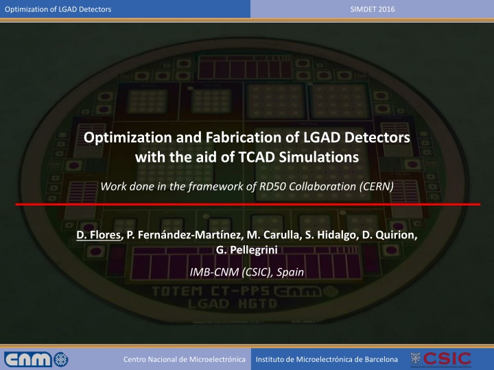
Optimization of LGAD Detectors SIMDET 2016 Optimization and Fabrication of LGAD Detectors with the aid of TCAD Simulations Work done in the framework of RD50 Collaboration (CERN) D. Flores, P. Fern ndez-Mart nez, M. Carulla, S. Hidalgo, D. Quirion, G. Pellegrini IMB-CNM (CSIC), Spain Centro Nacional de Microelectr nica Instituto de Microelectr nica de Barcelona
Optimization of LGAD Detectors SIMDET 2016 Outline 1. IMB-CNM Presentation 2. Introduction to Basic Simulation Procedures 3. LGAD Basic Detectors 4. Fitting Simulations and Process Technology 5. Improving Radiation Hardness 6. HGTD and CT-PPS Simulation and optimization 7. Conclusions Centro Nacional de Microelectr nica Instituto de Microelectr nica de Barcelona
Optimization of LGAD Detectors SIMDET 2016 IMB-CNM Presentation Public Research Organism that belongs to the Spanish Council for Scientific Research (CSIC) Located in Bellaterra, close to Barcelona (Spain) Devoted to Nano and Microelectronics Micro Nano Fabrication Facility (Clean Room) Departments: Micro and Nano Systems Systems Integration (Power Systems) STAFF (2013) 2013 Budget: 9.95 M External funding: 43.4 % Researchers 67 Ph.D. Students 25 Clean room 39 Project funding splitting: EU: National: 15 % Industrial contracts: 18 % 67 % Support services 28 Management & admin 16 TOTAL: 175 Centro Nacional de Microelectr nica Instituto de Microelectr nica de Barcelona
Optimization of LGAD Detectors SIMDET 2016 IMB-CNM Facilities Laboratories Characterization and test DC and RF (up to 8 GHz) Power devices Wafer testing IR Thermography Radiation testing Reverse Engineering Simulation CAD Mechanical Workshop Chemical sensors Bio-sensors Radiation sensors Optical sensors Clean Room 1.500 m2, class 100 to 10.000 Micro and nano fabrication technologies Three areas: Pure (CMOS) Noble metals allowed Nanoelectronics Processes 4'' complete 6' (no poly) Available technologies: CMOS, Power Devices (Si, SiC) MCM-D, MEMS/NEMS Bump bonding packaging Silicon micromachining Packaging 200 m2, class 1000 Centro Nacional de Microelectr nica Instituto de Microelectr nica de Barcelona
Optimization of LGAD Detectors SIMDET 2016 IMB-CNM Clean Room Images Centro Nacional de Microelectr nica Instituto de Microelectr nica de Barcelona
Optimization of LGAD Detectors SIMDET 2016 for: High Energy Physics Design, simulation, fabrication and test of radiation detectors Sincrotron 3D - Combined powder diffraction images 200 180 50 160 140 100 120 100 150 80 60 200 40 20 250 500 1000 1500 2000 2500 3000 3500 4000 4500 5000 5500 Dosimetry Medical Imaging Nuclear Physics Security Centro Nacional de Microelectr nica Instituto de Microelectr nica de Barcelona
Optimization of LGAD Detectors SIMDET 2016 III. FEM Simulations: SDevice Introduction to Basic Simulation Procedures: Sentaurus Device Centro Nacional de Microelectr nica Instituto de Microelectr nica de Barcelona
Optimization of LGAD Detectors SIMDET 2016 II. FEM Simulations: SDevice Sentaurus Device: Sdevice has not a graphical interface. Instructions are introduced from a command file (.cmd) Tool used for FEM Simulations Mixed Mode Device Mode Devices in the Circuit Files to Solve the Model File with Spice elements Physics Models Elements in the Circuit and their connections Types of Analysis: Quasistationary, Transient, ACCoupled Centro Nacional de Microelectr nica Instituto de Microelectr nica de Barcelona
Optimization of LGAD Detectors SIMDET 2016 III. FEM Simulations: SDevice Device Mode Simple Simulation: I-V curve on a Diode File { Plot Output = Diode_IV.log } Electrode { } Grid Current = Diode_IV.plt = Diode_IV.tdr = Diode_msh.tdr {Name= ElectrodeN Voltage = 0.0} {Name= ElectrodeN Voltage = 0.0} Diode_IV.cmd Physics { Math { Method=Pardiso Number_of_threads = 4 Stacksize=200000000 Extrapolate Derivatives AvalDerivatives RelErrControl Iterations=15 Notdamped=60 AreaFactor = 1 Temperature = 300 #Cylindrical Mobility ( Recombination ( EffectiveIntrinsicDensity (OldSlotboom) } DopingDependence eHighFieldSaturation hHighFieldSaturation Enormal CarrierCarrierScattering ) SRH (DopingDependence) Auger (withGeneration) Avalanche (UniBo Eparallel) Band2Band (Hurkx) ) BreakCriteria { Current (Contact = "ElectrodeN" maxval = 1e-8) } } Centro Nacional de Microelectr nica Instituto de Microelectr nica de Barcelona
Optimization of LGAD Detectors SIMDET 2016 III. FEM Simulations: SDevice Device Mode Simple Simulation: I-V curve on a Diode (Quasistationary) Plot { eCurrent/Vector hCurrent/Vector Current/Vector Potential ElectricField/Vector SpaceCharge eMobility hMobility eVelocity hVelocity DopingConcentration DonorConcentration AcceptorConcentration srhRecombination AugerRecombination AvalancheGeneration eAvalanche hAvalanche TotalRecombination } eDensity hDensity Diode_IV.cmd Solve { Coupled (Iterations=50) {Poisson} Coupled (Iterations=15) {Hole Poisson} Coupled (Iterations=15) {Electron Hole Poisson} QuasiStationary ( InitialStep = 1e-6 MaxStep = 0.01 MinStep = 1e-9 Goal {Name="ElectrodeN" Voltage=1000} Plot {Range = (0 1) Intervals=2} ) { Coupled {Hole Electron Poisson} Plot ( FilePrefix="IV_" Time=(0.01; 0.05; 0.1; 0.5) NoOverwrite ) } } Centro Nacional de Microelectr nica Instituto de Microelectr nica de Barcelona
Optimization of LGAD Detectors SIMDET 2016 III. FEM Simulations: SDevice Device Mode Simple Simulation: I-V curve on a Diode Diode_IV.plt Centro Nacional de Microelectr nica Instituto de Microelectr nica de Barcelona
Optimization of LGAD Detectors SIMDET 2016 III. FEM Simulations: SDevice Mixed Mode Simple Simulation: C-V curve on a Diode (AC Coupled) device Diode { Diode_CV.cmd Electrode { . . } System { Diode diodesystem ("ElectrodeN"=front "ElectrodeP"=0) Vsource_pset vn (front 0) {dc=0} File { Grid Current = "Diode_CV_1kHz.plt" Plot = "Diode_CV_1kHz.tdr" } } = "Diode_msh.tdr" File { Output ="Diode_CV_1kHz.log" ACExtract = "Diode_CV_AC_1kHz.plt" } Physics { ..... } Plot { ..... } } #End device Diode Centro Nacional de Microelectr nica Instituto de Microelectr nica de Barcelona
Optimization of LGAD Detectors SIMDET 2016 III. FEM Simulations: SDevice Mixed Mode Simple Simulation: C-V curve on a Diode (AC Coupled) Diode_CV.cmd Solve { Coupled (Iterations=50) {Poisson} Coupled (Iterations=15) {Hole Poisson} Coupled (Iterations=15) {Electron Hole Poisson} Coupled (Iterations=15) {Electron Hole Poisson Contact} QuasiStationary ( InitialStep = 1e-6 MaxStep = 1e-2 MinStep = 1e-7 Increment = 2 Decrement = 4 Goal {Parameter = vn.dc Voltage=100} ) { ACCoupled ( StartFrequency=1e3 EndFrequency=1e3 NumberOfPoints =1 Decade Iterations=15 Node (front) ACMethod=Blocked ACSubMethod("diodesystem")=ParDiSo ){ Poisson Electron Hole Contact Circuit} } } Centro Nacional de Microelectr nica Instituto de Microelectr nica de Barcelona
Optimization of LGAD Detectors SIMDET 2016 III. FEM Simulations: SDevice Mixed Mode Simple Simulation: C-V curve on a Diode (AC Coupled) Centro Nacional de Microelectr nica Instituto de Microelectr nica de Barcelona
Optimization of LGAD Detectors SIMDET 2016 III. FEM Simulations: SDevice Transient Simulation: Heavy Ion Impact Diode_HI.cmd Physics { ... HeavyIon ( Direction = (0,1) Location = (200, 0) Time = 1e-9 Length = [0 0.001 100 100.001] Wt_hi = [1.0 1.0 1.0 1.0] LET_f =[0 8.7e-6 8.7e-6 0] Gaussian PicoCoulomb ) } Solve { . Transient ( NewCurrentPrefix = "trans_" InitialTime = 0 FinalTime = 35e-9 MinStep = 1e-17 MaxStep = 1e-10 ){Coupled { Poisson Electron Hole Circuit } Plot (FilePrefix="TransHI_" Time=(0.5e-9; 1e-9; 2e-9; 5e-9; 10e-9) NoOverwrite) } } Centro Nacional de Microelectr nica Instituto de Microelectr nica de Barcelona
Optimization of LGAD Detectors SIMDET 2016 III. FEM Simulations: SDevice Transient Simulation: Heavy Ion Impact Centro Nacional de Microelectr nica Instituto de Microelectr nica de Barcelona
Optimization of LGAD Detectors SIMDET 2016 III. FEM Simulations: SDevice Transient Simulation: Laser Illumination Optics ( OpticalGeneration ( ComputeFromMonochromaticSource () TimeDependence ( WaveTime = (1e-9 1e-9) WaveTSigma = 50e-12 ) Scaling = 0 ) Excitation ( Wavelength = 0.8 *um Intensity = 0.06 *W/cm2 Window("L1") ( Origin = (200,0) XDirection = (1,0,0) Line (Dx = 10) ) Theta = 0 * Angle from positive y-axis ) OpticalSolver ( OptBeam ( LayerStackExtraction ( WindowName ="L1" WindowPosition = Center Mode = ElementWise ) ) ) ComplexRefractiveIndex (WavelengthDep (real imag)) ) Diode_Opt.cmd Solve { . Transient ( NewCurrentPrefix = "trans_" InitialTime = 0 FinalTime = 60e-9 MinStep = 1e-17 MaxStep = 1e-10 ){Coupled { Poisson Electron Hole Circuit } } } Centro Nacional de Microelectr nica Instituto de Microelectr nica de Barcelona
Optimization of LGAD Detectors SIMDET 2016 III. FEM Simulations: SDevice Transient Simulation: Laser Illumination Centro Nacional de Microelectr nica Instituto de Microelectr nica de Barcelona
Optimization of LGAD Detectors SIMDET 2016 III. FEM Simulations: SDevice Mixed Simulation with a more complicated circuit System { Set(ground=0) Vsource_pset V_bias (cathode ground) {dc=0} Diode diodesystem ("ElectrodeN"=cathode "ElectrodeP"=anode) Inductor_pset L_leak(anode ground){inductance=1e6} #CSF input capacitance Capacitor_pset C_in (anode ground){capacitance=1e-12} #CSF passive feedback network: Capacitor_pset C_csf (anode out) {capacitance=8e-15} Resistor_pset R_csf (anode out) {resistance=100e6} #CSA amp internal out resistence Resistor_pset R_sh(out ground){resistance=1} #CSA external capacitance Capacitor_pset C_out (out ground){capacitance=1e-12} Plot "CircuitCSF" (time() v(anode ground) v(out ground) v(anode out) i(L_leak anode) i(C_in anode) i(R_sh out) i(C_out out))} # Detector connected to a CSF (charge sensitive filter) #Vbias between ground and cathode #Detector between cathode and anode #C_in between anode and ground #CSF Passive network #L_leak between anode and ground #C_csf and R_csf between anode and outamp #R_outamp between outamp and ground Centro Nacional de Microelectr nica Instituto de Microelectr nica de Barcelona
Optimization of LGAD Detectors SIMDET 2016 III. FEM Simulations: SDevice Mixed Simulation with a more complicated circuit Centro Nacional de Microelectr nica Instituto de Microelectr nica de Barcelona
Optimization of LGAD Detectors SIMDET 2016 III. FEM Simulations: SDevice Simulation of the Radiation Effects Diode_Rad_IV.cmd Diode_Rad_CV.cmd Physics (material="Silicon") { Traps ( (Acceptor Level EnergyMid=0.42 fromCondBand Conc=2.3226E15 Randomize=0.29 eXsection=9.5E-15 hXsection=9.5E-14) #Conc=Fluence*1.1613 (Acceptor Level EnergyMid=0.46 fromCondBand Conc=1.8E15 Randomize=0.23 eXsection=5E-15 hXsection=5E-14 ) #Conc=Fluence*0.9 (Donor Level EnergyMid=0.36 fromValBand Conc=1.8E15 Randomize=0.31 eXsection=3.23E-13 hXsection=3.23E-14 ) #Conc=Fluence*0.9 ) } Physics (MaterialInterface="Oxide/Silicon") { # Traps (FixedCharge Conc=5e10 Charge(Conc=1.5e11) } ) Centro Nacional de Microelectr nica Instituto de Microelectr nica de Barcelona
Optimization of LGAD Detectors SIMDET 2016 III. FEM Simulations: SDevice Simulation of the Radiation Effects : I-V Simulation Centro Nacional de Microelectr nica Instituto de Microelectr nica de Barcelona
Optimization of LGAD Detectors SIMDET 2016 III. FEM Simulations: SDevice Simulation of the Radiation Effects : C-V Simulation Centro Nacional de Microelectr nica Instituto de Microelectr nica de Barcelona
Optimization of LGAD Detectors SIMDET 2016 IV. Additional Tools: SProcess Sentaurus Process Tool for emulating the technological steps of a fabrication process It allows emulating: - Deposition of layers of different materials - Localized etching of material with a mask - Ion implantation - Diffusion of the implanted species (thermal steps) - Oxide and epitaxial growth A specific mesh is created to solve the process emulation equations - Etc (almost any process you can perform in a real clean room) Usually, this mesh is not suitable for device simulation It is a powerful tool, that can faithfully reproduce the fabrication processes of a given clean room. Centro Nacional de Microelectr nica Instituto de Microelectr nica de Barcelona
Optimization of LGAD Detectors SIMDET 2016 IV. Additional Tools: SProcess Sentaurus Process: From a Foundry Point of View General Simulation flow Process Technology Simulation Re-meshing and adjustment FEM Simulation Regular use of Sprocess in a foundry (at least at IMB-CNM) 1stMode: From device performance to fabrication process - Combined SDE and Sdevice Simulations are necessary to obtain the desired performance - Sprocess simulation is carried out to determine the technological steps that provide the optimized performance 2ndMode: From fabrication process to device performance - A new or modified technological step is simulated with sprocess - The performance of the whole device is then analyzed with the aid of a SDE+Sdevice simulation Centro Nacional de Microelectr nica Instituto de Microelectr nica de Barcelona
Optimization of LGAD Detectors SIMDET 2016 III. FEM Simulations: SDevice LGAD Basic Detectors Centro Nacional de Microelectr nica Instituto de Microelectr nica de Barcelona
Optimization of LGAD Detectors SIMDET 2016 PiN Diode (No Gain) N+cathode P-type ( )substrate P+anode Abrupt N+P junction with trapezoidal electric field profile(linearly decreasingin the P substrate) Electrons are accelerated towards the N+region until they reach the saturationvelocity Since the electric field is much lower than Ecrit, electrons can not generatenew carriers (NO IMPACT IONIZATION AND NO GAIN) Centro Nacional de Microelectr nica Instituto de Microelectr nica de Barcelona
Optimization of LGAD Detectors SIMDET 2016 Pad Diode with internal Gain (LGAD) N+cathode P-type multiplication layer P-type ( )substrate P+anode GaussianN+P junction wherethe P-multiplication layer becomes completelydepleted at a very low reverse voltage Electrons are accelerated towards the N+region until they reach the saturationvelocity The electric field in the P layer is close to the Ecrit, value (IMPACT IONIZATION AND GAIN) Centro Nacional de Microelectr nica Instituto de Microelectr nica de Barcelona
Optimization of LGAD Detectors SIMDET 2016 Conditions for Gain Impact ionization requires a minimum electric field of 1e5 V/cm in the P layer Full depletion of the P-type substrateis neededto avoid recombination The Ecritvalue (~3e5 V/cm) can not be reachedin the N+P junction (reverse breakdown) Impact ionization region Electrons traveling at their saturation velocity (good for signal uniformity) Centro Nacional de Microelectr nica Instituto de Microelectr nica de Barcelona
Optimization of LGAD Detectors SIMDET 2016 Design of the P-Multiplication Region Doping profile of the P-multiplication layer is critical 1D Simulation @ Pad Centre Gain/VBDtrade-off If implant dose increases: Gain increases VBDdecreases Small modifications in the Boron implant dose induce great changes in Gain and VBD Centro Nacional de Microelectr nica Instituto de Microelectr nica de Barcelona
Optimization of LGAD Detectors SIMDET 2016 Design of the Edge Termination The optimization of the edge termination is ruled by the electric field at the multiplication layer (not by the maximum voltage capability, as in the case of power devices) P-Multiplication layer Correlated values P-Substrate Centro Nacional de Microelectr nica Instituto de Microelectr nica de Barcelona
Optimization of LGAD Detectors SIMDET 2016 Edge Termination: Why is needed? The N+shallow contact and the P-multiplication layers have to be locally created witha lithographymask The electric field at the curvature of the N+/P junction is much higher than that of the plane junction (where Gain is needed) Avalanche at the N+/P curvature at a very low reverse voltage (premature breakdown) Shallow N+and P-multiplication layers self aligned High electric field peak at the curvature Centro Nacional de Microelectr nica Instituto de Microelectr nica de Barcelona
Optimization of LGAD Detectors SIMDET 2016 Edge Termination with N+Extension The N+shallow diffusion is used to extendthe N+beyond the edge of the multiplication layer Enhanced Phosphorous diffusion in the very low doped substrate (increased curvature radius and voltage capability) The electric field rapidly increases at the plain junction (multiplication) At high reverse voltage the electric peak at the extended N+diffusion leads to breakdown Avalanche Multiplication Centro Nacional de Microelectr nica Instituto de Microelectr nica de Barcelona
Optimization of LGAD Detectors SIMDET 2016 Edge Termination with Junction Termination Extension Junction TerminationExtension (JTE) with an additional deepN diffusion Additional photolithographic step with high energy Phosphorous implantation A field platecan also be implementedfor additional electric field smoothing Field Plate N+cathode P-type multiplication layer JTE diffusion P-type substrate P+anode Centro Nacional de Microelectr nica Instituto de Microelectr nica de Barcelona
Optimization of LGAD Detectors SIMDET 2016 Edge Termination with Junction Termination Extension Deep N diffusion with high curvatureradius (long anneal process) Reduced electric field peak at the JTE diffusion Highest electric field at the plane junction (gain control) VBD plane< VBD JTE(Gain control) Multiplication and avalanche control Centro Nacional de Microelectr nica Instituto de Microelectr nica de Barcelona
Optimization of LGAD Detectors SIMDET 2016 Design of the Device Periphery Full depletion below 100 V reverse bias Fast lateral depletion of the low doped substrate. A deep P+diffusion P stop- is needed in the die peripheryto avoid the depletion region reaching the unprotected edge Centro Nacional de Microelectr nica Instituto de Microelectr nica de Barcelona
Optimization of LGAD Detectors SIMDET 2016 What about the Inherent Positive Oxide Charges? Field oxides grown in wet conditions (H2+O2) typically with a positive charge density of 5e10 cm-2 x Surface inversion and modificationof the depletion region, reaching the deep P-Stop peripheral diffusion Surface inversion + fast depletion + electric field peak at deep P-stop + SURFACE LEAKAGE CURRENTS Centro Nacional de Microelectr nica Instituto de Microelectr nica de Barcelona
Optimization of LGAD Detectors SIMDET 2016 How to Protect the Surface, Limiting the Current Leakage? Oxide positive charges create a surface inversion layer (electron path towards the cathode electrode, masking the charge collection when used as a detector) A shallow P-type diffusion (P-Spray) can be used to compensatethe surface inversion A deep P+diffusion can be placed close to the JTE to eliminate the electron surface current Blanket Boron implantation Same Boron implantation Centro Nacional de Microelectr nica Instituto de Microelectr nica de Barcelona
Optimization of LGAD Detectors SIMDET 2016 How to Protect the Surface, Limiting the Current Leakage? An additional N-type collecting ring is implemented by using the deep JTE diffusion The N ring has to be placedclose to the JTE to avoid a prematurebreakdownat the JTE The P-spray diffusion has to be efficient (to avoid short circuit through the inversion layer) The voltage capability is not degraded since the junction to be protected is now the right edge of the addedring (identical than the JTE) P N N N+ N+ P- Multiplier Junction Overlap Collector Ring P+ Centro Nacional de Microelectr nica Instituto de Microelectr nica de Barcelona
Optimization of LGAD Detectors SIMDET 2016 Simulation of the Irradiated Devices Curves @ 600 V No Irradiated Irradiated. eq = 1 x 10¹⁵ High Electric Field peak at the junction Irradiation Trap Model (Perugia Model) Acceptor; E= Ec+ 0.46 eV; =0.9 Acceptor; E= Ec+ 0.42 eV; =1.613 Acceptor; E= Ec+ 0.10 eV; =100 Donor; E= Ev- 0.36 eV; =0.9 PiN: electric field strength at the junction increases after irradiation e = 5 x 10-15 e = 2 x 10-15 e = 2 x 10-15 e = 2.5 x 10⁻¹⁴ h = 2.5 x 10⁻¹⁵ h = 5 x 10-14 h = 2 x 10-14 h = 2.5 x 10⁻¹⁵ LGAD: electric field strength at the junction is almost equal after irradiation Impact Ionization Model (Univ. of Bolonia) Centro Nacional de Microelectr nica Instituto de Microelectr nica de Barcelona
Optimization of LGAD Detectors SIMDET 2016 III. FEM Simulations: SDevice Fitting Simulations and Process Technology Centro Nacional de Microelectr nica Instituto de Microelectr nica de Barcelona
Optimization of LGAD Detectors SIMDET 2016 Conventional LGAD Detector Process Set-up Integrate a pad detector for tracking applications with internal gain (5-10) The leakage current has to be as low as possible Surface inversion is always a challenge in extremely low doped substrates (P-Spray, P-Stop and other structures have to be used Although a double Boron and Phosphorous implantation is something quite simple (through a screen oxide), a precise control is mandatory and repeatability is the key point for production purposes Silvaco platform is preferred for process simulation when dealing with Silicon technology Sentaurus platform is preferred for performance and irradiation effects simulation SEM inspection and SIMs profiles are useful tools for technology stabilization -3- Centro Nacional de Microelectr nica Instituto de Microelectr nica de Barcelona
Optimization of LGAD Detectors SIMDET 2016 Conventional LGAD Process Technology Several fabrication runs to optimize the performance of the LGAD devices. High resistivity P-type substrate, 200 & 300 m thick Wafers with different P-layer doping doses Wafers with PiN diodes included for reference Front view of the wafer Metal grid Back view of one LGAD detector 7 Photolithographic levels More than 80 Technological Steps Average fabrication time: 3 moths Centro Nacional de Microelectr nica Instituto de Microelectr nica de Barcelona
Optimization of LGAD Detectors SIMDET 2016 Fabricated Prototypes DR SiO2/Si3N4 Passivation Metal N-Type Diffusion (JTE) P-type multiplication layer Centro Nacional de Microelectr nica Instituto de Microelectr nica de Barcelona
Optimization of LGAD Detectors SIMDET 2016 Optimization of LGAD Electrical Simulations 1STStep: The Doping profile from process technology simulation is compared with the experimental SIMs values. A new Doping profile for electrical simulation is then obtained. V.Gkougkousis, LGAD Dopng Profiles, 27th RD50 Workshop, CERN, December 2015 Centro Nacional de Microelectr nica Instituto de Microelectr nica de Barcelona
Optimization of LGAD Detectors SIMDET 2016 Optimization of LGAD Electrical Simulations Dop_PWell Dop_Junction Dop_Psub tNPlus tPWell 5E+16 3E+16 5.5E+11 1,03 4,9 Centro Nacional de Microelectr nica Instituto de Microelectr nica de Barcelona
Optimization of LGAD Detectors SIMDET 2016 Optimization of LGAD Electrical Simulations 2ndStep: The new doping profile is validated by C(V) simulations and experimental data Foot Zoom VFD =70V ?~0.5? V=30V ZOOM -5- Centro Nacional de Microelectr nica Instituto de Microelectr nica de Barcelona
Optimization of LGAD Detectors SIMDET 2016 Optimization of LGAD Electrical Simulations 3rdStep: The Gain Simulation is compared with the experimental Gain (measured with a tri- alfa source at IMB-CNM), as well as with the experimental MIP data (measured at CERN). Gain @ 700V 4.4 Gain @ 700V 4.2 Otero.S; Characterization of LGAD Sensors CNM Run7859 RD50 December 2015 -6- Centro Nacional de Microelectr nica Instituto de Microelectr nica de Barcelona
Optimization of LGAD Detectors SIMDET 2016 Optimization of LGAD Electrical Simulations (Silvaco & Synopsys) Dop_PWell 5E+16 7E+16 9E+16 Dop_NPlus 3.8E+19 3.5E+19 3.5E+19 Dop_Junction 3E+16 4.5E+16 3.8E+16 Dop_Psub 5.5E+11 5.5E+11 5.5E+11 tNPlus 1.03 1.1 1.08 tPWell 4.9 5.67 4.17 Synopsys (SIMS Fit) Silvaco full.cpl Silvaco Fermi Centro Nacional de Microelectr nica Instituto de Microelectr nica de Barcelona
Optimization of LGAD Detectors SIMDET 2016 Optimization of LGAD Electrical Simulations Diffusion Models: All diffusion models (Fermi, two dimensional or fully coupled model) follow the same generic mathematical form of a continuity equation. Second order Fick s Equation ??? ??= ???+ ? (1) At any given temperature, a finite number of dopant-defect pairs is present. This fraction is responsible for the redistribution of dopant atoms. Fermi Model: The Fermi Model assumes that point defects are in thermodynamic equilibrium. There is no difference between Interstitials or Vacancies and Vacancies with different charge states interact with impurities independently. The diffusion coefficient in extrinsic silicon is described by 2 ? ? ? 0+ ?? + = ? = ?? + ?? + ?? (2) ?? ?? ?? Full coupled Model: Substitutional impurities are assumed to move both via vacancy-assisted diffusion with a fraction ??= 1 ??and via interstitial-assisted diffusion with a fraction ??. By default ??= 0.94. The model is based in non-equilibrium of point defects concentration. The coupled equations for impurities and point defects must be solved, because impurities continue to have dynamic interactions with point defects during annealing. Centro Nacional de Microelectr nica Instituto de Microelectr nica de Barcelona
