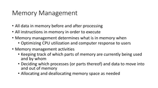
Memory Organization in Computer Systems


Computer Organization
1
Memory
Organization
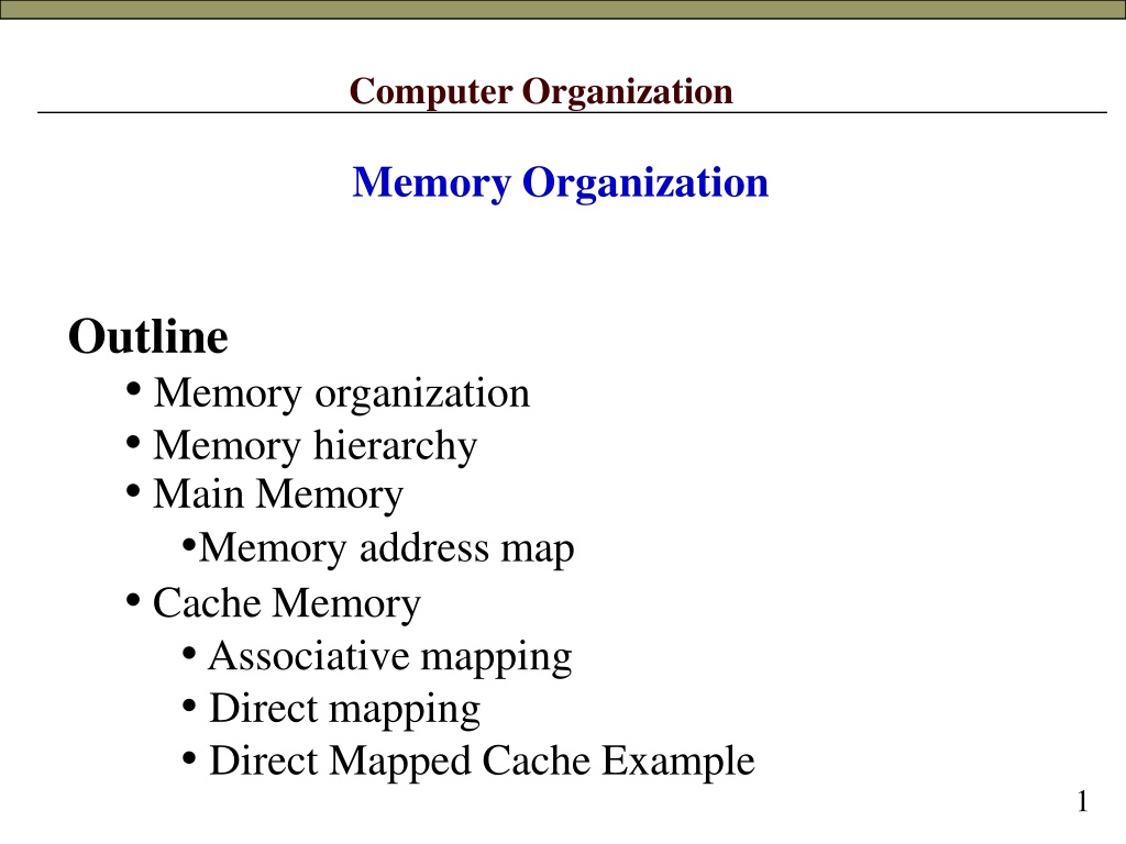
Outline
•
Memory
organization
•
Memory
hierarchy
•
Main
Memory
•
Memory
address
map
•
Cache
Memory
•
Associative
mapping
•
Direct
mapping
•
Direct
Mapped
Cache
Example
Memory
Organization
(1/6)
2
Recall:
Information
is
stored
in
the
memory
as
a
collection
of bits.
Collection
of bits
are
stored
or
retrieved
simultaneously
is
called
a word.
Number
of
bits
in
a
word
is
called
word
length.
Word
length
can
be
16
to
64
bits.
Another
collection
which
is
more
basic
than
a
word:
Collection
of 8
bits
known
as
a
“byte”
Bytes are grouped into
words,
word length can also be
expressed
as
a
number
of
bytes
instead
of
the
number
of
bits:
Word
length
of
16
bits,
is
equivalent
to
word length
of
2
bytes.
Words
may
be
2
bytes
(older
architectures),
4
bytes
(current
architectures),
or
8+
bytes
(modern
architectures).
Memory
Organization
(2/6)
3
Accessing
the
memory
to obtain
information
requires specifying
the
“address”
of the
memory
location.
Recall
that
a
memory
has
a
sequence
of
bits:
Assigning
addresses
to
each
bit
is
impractical
and
unnecessary.
Typically,
addresses
are
assigned
to
a
single
byte.
“Byte
addressable
memory”
Suppose
k
bits
are
used
to
hold
the
address
of
a
memory
location:
Size
of
the
memory
in
bytes
is
given
by: 2^k
where
k
is
the
number
of
bits
used
to
hold
a
memory
address.
E.g.,
for
a
16-bit
address,
size
of
the
memory
is
2^16=
65536
bytes
What
is
the
size
of
the
memory
for
a
24-bit
address?
Memory
Organization
(3/6)
Memory
is viewed
as
a
sequence
of
bytes
.
Address
of
the first
byte
is
0
Address
of
the last
byte
is
2
k
–
1.
Where
k is the number
of
bits used
to
hold
memory
address.
E.g.
when
k
=
16,
Address
of
the
first
byte
is
0
Address
of
the
last
byte
is
65535
Byte
0
Byte
2
k
-1
4
Last
word
(Word
#?)
starts
at
Byte#?
5
Memory
Organization
(4/6)
W
o
r
d
#?
W
o
r
d
#
0
W
o
r
d
#
1
Consider
a
memory
organization:
16-bit
memory
addresses
Size
of
the
memory
is =
2^16
=65536
B
[Byte
0..Byte
65535]
Word
length
is
4
bytes
Number
of
words
=
Memory size(bytes
)
=
?
Word
length(bytes)
=
16384
words
Word
#0
starts
at
Byte
#0.
Word
#1
starts
at
Byte
#4.
Memory
Organization
(5/6)
W
or
d
#1
W
o
r
d
#16383
MAR
MDR
Addr
65532
MAR
register
contains
the
address of
the
memory
location
addressed
6
MDR
contains
either the
data
to
be
written to
that
address or
read
from
that
address.
W
or
d
#0
Memory
Organization
(6/6)
7
Memory
read
or
load:
Place
address
of
the
memory
location
to
be
read
from,
into
MAR.
Issue
a
Memory_read
command
to
the
memory.
Data
read
from
the
memory
is
placed
into
MDR
automatically
(by control
logic).
Memory
write
or
store:
Place
address
of
the
memory
location
to
be
written
to
into
MAR.
Place
data
to
be
written
into
MDR.
Issue
Memory_write
command
to
the
memory.
Data
in
MDR
is
written
to
the
memory
automatically
(by
control
logic).
Memory
Hierarchy
(1/3)
8
The
memory
unit
is
then an essential
component
in any
digital
computer
since
it
is
needed
for
storing
programs
and
data.
The
memory
unit
that
communicates
directly
with
the
CPU
is
called
the
main
memory
.
Devices
that
provide
backup
storage
are
called
auxiliary
memory
(Magnetic
disks
and
tapes).
Only
programs
and
data
currently
needed
by
the
processor
reside
in
main
memory
.
There
is
a special very – thigh – speed
memory
called
cache
employed
between the
CPU
&
main memory
to
compensate
for
the
mismatch
in
operating
speeds.
Memory
Hierarchy
(2/3)
9
Cache
memory
is sometimes used
to increase the speed of
processing by
making
current
programs
and data available to
the
CPU
at
a
rapid
rate
(extremely
fast),
Whose
access
time
is
close
to processor
logic
clock
cycle
time.
It used for storing
segments of programs
currently being
executed
in
the
CPU
and
temporary
data
frequently
needed.
The
cache
organization
is then
concerned
with
the
transfer
of
information
between
a
main
memory
and CPU.
The part of the
computer system
that supervises the flow of
information
between auxiliary
memory
and
main
memory
is
called
the
memory
management
system.
Memory
Hierarchy
(3/3)
Memory
hierarchy
in
a
computer
system
Auxiliary
memory
(Secondary)
Magnetic
tapes
Magnetic
disks
I/O
Processor
CPU
Main
m
e
m
ory
Cache
m
e
m
ory
10
Main
Memory (1/4)
11
The
main
2
types
of
main
memory
are:
RAM
which
is
to
used
to
refer
to
a
read/write
random-access
memory
ROM which
is
to
used to
refer
to
a
read
only
random-access
memory
.
Integrated
circuit
RAM
chips
are
available
in
two
possible
operating
modes,
static
and
dynamic
.
The
static
RAM
consists
essentially
of
internal
flip–flops
that
store the binary
information,
the stored
information remains
valid
as
long
as
power is
applied
to the
unit
.
The
dynamic
RAM
stores the
binary
information
in
the
form
of
electric
charges
that
are
applied
to
capacitors.
Main
Memory
(2/4)
12
The
stored
charge
on
the
capacitors
tend
to
discharge
with
time
and
the
capacitors
must
be
periodically
recharged
by
refreshing
the
dynamic
memory.
The
dynamic
RAM
offers
reduced
power
consumption
and
larger
storage
capacity
in
single
memory
chip.
But
the
static
RAM
is
easier
to
use
and
has
shorter read
and
write
cycles.
ROM
is
used
for storing
programs
that are
permanently
resident
in
the
computer.
The
ROM
portion
of
main
memory
is
needed
for
storing
an
initial
program
called
a
bootstrap
loader.
The
bootstrap
loader
is
a
program
whose
function
is
the
start
the
computer
software
operating
when
power
is
turned
on.
13
Main
Memory
(3/4)
RAM
and
ROM
chips
are
available
in
a
variety
of
sizes
.
For example
of
a
1024
x
8
memory
can
be
constructed
with
128
x
8
RAM
chips
and
512
x
8
ROM
chips.
8-bit
data
bus
Chip
select
1
Chip
select
2
Read
Write
7-bit
address
14
Main
Memory
(4/4)
8-bit
data
bus
C
S
1
C
S
2
512
X8
ROM
AD9
Chip
select
1
Chip
select
2
9-bit
address
The
data
bus
can
only
be
in
an
output
mode.
When
chip
is
enabled
by
the
2
select
inputs,
the
byte
selected
by
the
address
lines
appears
on
the
data
bus
Main
Memory:
Memory
address
map
(1/4)
15
Memory
address
map
The
addressing
of
memory
can
be
established
by
means
of a
table
, called a memory
address
map
,
that specifies the
memory
address
assigned to
each chip
.
For
example,
assume
that
a
computer
system
needs
512
bytes
of
RAM
and 512
bytes
of
ROM.
The
memory
address
map
for
this
configuration
is
shown
in
table
following
table.
Main
Memory:
Memory
address
map
(2/4)
16
Memory
Address
Map
for
Microprocomputer
17
Main Memory:
Memory
address
map
(3/4)
Although
there
are
16
lines
in
the
address
bus,
the
table
shows
only 10 lines
because
the other 6 are not used in this
example
and
are
assumed
to
be
zero.
The
small
x's
under the
address
bus
lines
designate
those
lines
that
must
be
connected
to
the
address
inputs
in
each
chip.
The
RAM
chips
have
128
bytes
and
need
7
address
lines
.
The
ROM
chip
has
512
bytes
and
needs
9
address lines
.
The
x's
are
always
assigned
to
the
low
– order
bus
lines
:
lines
1
through
7
for
the RAM
and
lines
1
through
9
for
the
ROM.
The
distinction
between
a
RAM
and
ROM
address
is
done
with
another
bus
line.
This
can
be
done
by
choosing
line
10
for
this
purpose
.
18
Main
Memory
:
Memory
address
map
(4/4)
C
S1
CS2
51
2
X
8
ROM
AD9
CS1
CS2
RD
128X8
WR
RAM
2
AD7
CS1
CS2
RD
128X8
WR
AM
1
AD7
C
S
1
C
S2
RD
128X8
WR
RAM
4
AD7
CS1
CS2
RD
128X8
WR
RAM
3
AD7
CPU
16
–
11 10
9
8
7
-1
RD
WR
Data
bus
Decoder
3
2
1
0
D
a
t
a
Memory
address
map
&
Connection
to
CPU
Cache
Memory
(1/5)
19
Analysis of a large
number
of typical
programs has shown
that
the
references
to
memory
at
any
given
interval
of
time
tent
to
be
confined
within
a
few
localized
areas
in
memory.
This
phenomenon
is
known
as
the
property
of
locality
of
reference.
If
the
active
portions
of
the
program
and
data
are
placed
in
a
fast
small
memory,
the average
memory
access
time
can be reduced,
thus
reducing
the
total
execution
time
of the
program
.
Cache
Memory
(2/5)
20
The
performance
of cache
memory
is
frequently
measured
in
terms
of
a
quantity
called
hit
ratio
.
When
the
CPU refers
to
memory
and finds the word in cache, it
is
said
to
produce
a
hit.
If the
word
is
not found
in
cache
,
it is
in
main
memory
and
it
counts
as
a
miss
.
No.
of
hits
=
number
of
successful
cache memory
references.
Misses
=
number
of
unsuccessful
cache
memory
references.
The
ratio
of
the
number
of
hits
divided
by
the
total
CPU
references
to
memory
(hits
plus
misses)
is
the
hit
ratio
,
[Hit
ratio
=
hits/
(hits
+
misses)]
Average
access
time
for
a
memory
with
a
single-level
cache
formula.
A
=
C
+
(1-
H
)
M
A
is
the
average
access
time
of
the
system
M
is
the
access
time
of
the
main
memory
C
is
the
access
time
of
the
cache
H
is
the
percent
of
accesses
that
are
satisfied
from
the
cache.
Example,
a
computer with
cache access
time
of
100 ns
,
a
main
memory
access
time
of 1000
ns
, and a hit ratio of 0.9,
produces
an
average
access
time
of
200
ns.
21
Cache
Memory
(3/5)
22
Cache
Memory
(4/5)
The transformation of data from
main memory
to
cache
memory
is
referred
to
as
a
mapping
process
.
Three types of mapping procedures are of practical
interest when considering
the
organization of
cache
memory.
Direct
mapping.
Associative
mapping.
Set-associative
mapping
.
23
Cache
Memory
(5/5)
Small
amount
of
fast
memory
Sits
between
normal
main
memory
and
CPU
May
be
located
on
CPU
chip
or
module
For
every
word
stored
in
cache,
there
is
a
duplicate
copy
in
main
memory.
To
illustrate
these
3
mapping
procedures
,
a specific
example
of
a
memory
organization
will
be
used
as
shown.
Main
Memory
32k
X
12
C
P
U
Cache
Memory
512
X
12
Example
of
Cache
Memory
Bloc
transfer
Word
transfer
Cache
Memory
:
Associative
Mapping
(1/2)
The
fastest
and
most
flexible
cache
organization
uses
an
Associative
Mapping
,
as
illustrated
in
the
following
diagram.
Associative
mapping
cache
(all
numbers in
octal)
CPU
address
(15
bits
)
Argument
register
24
Cache
Memory:
Associative
Mapping
(2/2)
25
The
associative
memory
stores
both
the
address
and
content
(
data
)
of
the
memory
word.
This
permits
any
location
in
cache
to
store
any
word
from
main
memory.
A
CPU
address
of
15
bits
is
placed
in
the
argument
register
and the
associative memory
is
searched for a
matching
address.
If
the
address
is found
,
the
corresponding
12-
bit
data
is
read
and
sent
to the
CU.
If no
match occurs,
the
main
memory
is
accessed for the
word.
The
address-data
pair
is
then
transferred
to
the
associative
cache
memory
based
on a
replacement
algorithm
.
26
Cache
Memory:
Direct
mapping
(1/5)
Associative
memories
are
expensive
compared
to
random access
memories, which
can
be used
for the
cache,
because
of
the
added
logic
associated
with each
cell.
This
organization
is
shown
in
the
following
diagram:
6
bits
9
bits
32
k
X12
Main
memory
Address=
15
bits
Data=
12
bits
512
X12
Cache
memory
Address=
9
bits
Data=
12
bits
Tag
Index
77
777
00
000
Octal
A
d
dress
Octal
Address
000
777
27
Cache
Memory:
Direct
mapping
(2/5)
000
777
data
Index
address
Tag
Cache
memory
Memory
address
00000
00777
01000
01777
02000
02777
Memory
data
Main
memory
1.
Direct
mapping
cache
Organization:
Block
size
of
one
word
(simplest
cache)
Cache
Memory:
Direct
mapping
(2/5
bis)
Index
determines
block
in
cache
If
number
of
cache
blocks
is
power
of
2,
then cache index is just the lower
n
bits
of
memory
address
Tag
Index
Address
Main
Memory
8
9
10
11
12
13
14
15
1
0
0
0
10
01
1
0
1
0
1
0
1
1
1
1
0
0
1
1
0
1
1
1
1
0
1
1
1
1
4-Block
Direct
Mapped
Cache
C
a
che
Index
0
1
2
3
00
01
10
11
28
Cache
Memory:
Direct
mapping
(3/5)
2.
Direct
mapping
cache Organization:
Block
size
of
eight
words
Index
Tag
Data
Block
0
Block
1
Block
63
6
bits
6
bits
3
bits
Index
29
Cache
Memory:
Direct
mapping
(3/5
bis)
If
block
size
>
1
word
,
rightmost
bits
of
index
are
really
the
offset
of
a
word
(possibly
byte
number)
within
the
indexed
block
oooo
Tag
to
check
if
have
correct
block
ttttttttttttttttt
iiiiiiiiii
Word
offset
within
block
Index
to
select
block
30
Cache
Memory:
Direct
mapping
(4/5)
31
The
CPU
address
of
15
bits
is
divided
into
two
fields
.
The
9
least
significant
bits
constitutes
the
index
field
and
the
remaining
6
bits
form
the
tag
field
.
The
number
of bits
in the
index
field
=
the
number
of
address
bits
required
to
access
the
cache
memory.
In the
general
case
,
there
are
2^
k
words
in
cache
memory
and
2^
n
words
in
main
memory
. The
n
-bits
memory
address
is
divided
into
two
fields:
k
bits
for
the
index
to access
the
cache
,
n
-
k
bits
for
the
tag
field
.
The
direct
mapping
cache
organization
uses:
The
n
-bit
address
to
access
the
main
memory,
And
the
k-bit
index
to
access
the
cache.
32
Cache
Memory:
Direct
mapping
(5/5)
Each
word
in
cache
consists
of
the
data
word
and
its
associated
tag
.
When
the
CPU
generates
a
memory
request
:
The
index
field
is
used
for
the
address
to
access
the
cache
.
The
tag
field
of
the
CPU
address
is compared with
the
tag in the
word
read
from
the cache
. If the two tags,
match
, there
is
a
hit
and the desired data word
is
in
cache.
If
there
is
no
match,
there
is
a miss
and
the
required
word
is read
from
main
memory.
It
is
then
stored
in
the
cache
together
with
the
new
tag
,
replac
i
ng
the
previous
valu
e
.
Direct
Mapped
Cache
Example
33
Direct
mapped
–
each
memory
block
can
occupy
one
and
only
one
cache block
Example:
Cache
block
size:
16
words
Memory
=
64K
(4K
blocks)
Cache
=
2K
(128
blocks)
Memory
block
n
occupies
cache
block
(
n
mod
128)
Consider address
$2EF4
001011101111 0100
block:
$2EF
=
751
word:
4
Cache:
00101
1101111
0100
tag:
5
block: 111
word:
4
Direct
Mapped
Cache
Example
34
Information stored in computer memory is in the form of bits grouped into bytes and words. Memory is accessed using addresses with byte-addressable memory being common. Different memory organizations and address mappings play a key role in managing data efficiently. Explore the basics of memory organization, word lengths, byte grouping, memory addressing, and more to understand how data is stored and retrieved in computer systems.

Download Presentation

Please find below an Image/Link to download the presentation.
The content on the website is provided AS IS for your information and personal use only. It may not be sold, licensed, or shared on other websites without obtaining consent from the author.If you encounter any issues during the download, it is possible that the publisher has removed the file from their server.
You are allowed to download the files provided on this website for personal or commercial use, subject to the condition that they are used lawfully. All files are the property of their respective owners.
The content on the website is provided AS IS for your information and personal use only. It may not be sold, licensed, or shared on other websites without obtaining consent from the author.
E N D
Presentation Transcript
Computer Organization Memory Organization Outline Memory organization Memory hierarchy Main Memory Memory address map Cache Memory Associative mapping Direct mapping Direct Mapped Cache Example 1
Memory Organization (1/6) Recall: Information is stored in the memory as a collection of bits. Collection of bits are stored or retrieved simultaneously is called a word. Number of bits in a word is called word length. Word length can be 16 to 64 bits. Another collection which is more basic than a word: Collection of 8 bits known as a byte Bytes are grouped into words, word length can also be expressed as a number of bytes instead of the number of bits: Word length of 16 bits, is equivalent to word length of 2 bytes. Words may be 2 bytes (older architectures), 4 bytes (current architectures), or 8+ bytes (modern architectures). 2
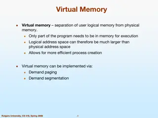
Memory Organization (2/6) Accessing the memory to obtain information requires specifying the address of the memory location. Recall that a memory has a sequence of bits: Assigning addresses to each bit is impractical and unnecessary. Typically, addresses are assigned to a single byte. Byte addressable memory Suppose k bits are used to hold the address of a memory location: Size of the memory in bytes is given by: 2^k where k is the number of bits used to hold a memory address. E.g., for a 16-bit address, size of the memory is 2^16= 65536 bytes What is the size of the memory for a 24-bit address? 3
Memory Organization (3/6) Byte0 Memory is viewed as a sequence of bytes. Address of the first byte is 0 Address of the last byte is 2k 1. Where k is the number of bits used to hold memory address. E.g. when k = 16, Address of the first byte is 0 Address of the last byte is 65535 Byte 2k-1 4
Memory Organization (4/6) Consider a memory organization: 16-bit memory addresses Size of the memory is = 2^16 =65536 B [Byte 0..Byte 65535] Word length is 4 bytes Byte 0 Byte 1 Byte 2 Byte 3 Byte 4 Word #0 Word #1 Number of words = Memory size(bytes) = ? Word length(bytes) =16384 words Word #0 starts at Byte #0. Word #1 starts at Byte #4. Byte 65532 Byte 65533 Byte 65534 Byte 65535 Word #? Last word (Word #?) starts at Byte#? 5
Memory Organization (5/6) Byte 0 Byte 1 Byte 2 Byte 3 Byte 4 Word #0 MAR MDR Word #1 MAR register contains the address of the memorylocation addressed Byte 65532 Byte 65533 Byte 65534 Byte 65535 Word #16383 Addr65532 MDR contains either the data to be written to that address or read from that address. 6
Memory Organization (6/6) Memory read or load: Place address of the memory location to be read from, into MAR. Issue a Memory_read command to the memory. Data read from the memory is placed into MDR automatically (by control logic). Memory write or store: Place address of the memory location to be written to into MAR. Place data to be written into MDR. Issue Memory_write command to the memory. Data in MDR is written to the memory automatically (by control logic). 7
Memory Hierarchy (1/3) The memory unit is then an essential component in any digital computer since it is needed for storing programs and data. The memory unit that communicates directly with the CPU is called the main memory. Devices that provide backup storage are called auxiliary memory (Magnetic disks and tapes). Only programs and data currently needed by the processor reside in main memory. There is a special very thigh speed memory called cache employed between the CPU & main memory to compensate for the mismatch in operating speeds. 8
Memory Hierarchy (2/3) Cache memory is sometimes used to increase the speed of processing by making current programs and data available to the CPU at a rapid rate (extremely fast), Whose access time is close to processor logic clock cycle time. It used for storing segments of programs currently being executed in the CPU and temporary data frequently needed. The cache organization is then concerned with the transfer of information between a main memory and CPU. The part of the computer system that supervises the flow of information between auxiliary memory and main memory is called the memory management system. 9
Memory Hierarchy (3/3) Memory hierarchy in a computer system Auxiliary memory (Secondary) Magnetic tapes Main memory I/O Processor Magnetic disks Cache memory CPU 10
Main Memory (1/4) The main 2 types of main memory are: RAM which is to used to refer to a read/write random-access memory ROM which is to used to refer to a read only random-access memory. Integrated circuit RAM chips are available in two possible operating modes, static and dynamic . The static RAM consists essentially of internal flip flops that store the binary information, the stored information remains valid as long as power is applied to the unit. The dynamic RAM stores the binary information in the form of electric charges that are applied to capacitors. 11
Main Memory (2/4) The stored charge on the capacitors tend to discharge with time and the capacitors must be periodically recharged by refreshing the dynamic memory. The dynamic RAM offers reduced power consumption and larger storage capacity in single memory chip. But the static RAM is easier to use and has shorter read and write cycles. ROM is used for storing programs that are permanently resident in the computer. The ROM portion of main memory is needed for storing an initial program called a bootstrap loader. The bootstrap loader is a program whose function is the start the computer software operating when power is turned on. 12
Main Memory (3/4) RAM and ROM chips are available in a variety of sizes. For example of a 1024 x 8 memory can be constructed with 128 x 8 RAM chips and 512 x 8 ROM chips. CS1 Chip select 1 Chip select 2 Read Write 7-bit address 8-bit data bus CS2 RD 128X8 WR RAM AD7 Memory function Stateof data bus CS1 CS2 RD WR 0 0 1 1 1 1 0 1 0 0 0 1 x x 0 0 1 x x x 0 1 x x Inhibit Inhibit Inhibit Write Read Inhibit High-impedance High-impedance High-impedance Inputdatato RAM Outputdatafrom RAM High-impedance 13
Main Memory (4/4) CS1 CS2 Chip select 1 Chip select 2 8-bit data bus 512X8 ROM 9-bit address AD9 CS1 CS2 Memoryfunction Stateof data bus 0 0 1 1 0 1 0 1 Inhibit Inhibit Read Inhibit High-impedance High-impedance Outputdatafrom ROM High-impedance The data bus can only be in an output mode. When chip is enabled by the 2 select inputs, the byte selected by the address lines appears on the data bus 14
Main Memory: Memory address map (1/4) Memory address map The addressing of memory can be established by means of a table , called a memory address map, that specifies the memory address assigned to each chip. For example, assume that a computer system needs 512 bytes of RAM and 512 bytes of ROM. The memory address map for this configuration is shown in table following table. 15
Main Memory: Memory address map (2/4) MemoryAddress Map for Microprocomputer Addressbus 8 7 6 5 10 9 4 3 2 1 Component Hexadecimaladdress RAM 1 RAM 2 RAM 3 RAM 4 ROM 0000-007F 0080-00FF 0100-017F 0180-01FF 0200-03FF 0 0 0 0 1 0 0 1 1 X X X X X 0 X X X 1 X X X 0 X X X 1 X X X X X X X X X X X X X X X X X X X X X X X 16
Main Memory: Memory address map (3/4) Although there are 16 lines in the address bus, the table shows only 10 lines because the other 6 are not used in this example and are assumed to be zero. The small x's under the address bus lines designate those lines that must be connected to the address inputs in each chip. The RAM chips have 128 bytes and need 7 address lines. The ROM chip has 512 bytes and needs 9 address lines. The x's are always assigned to the low order bus lines: lines 1 through 7 for the RAM and lines 1 through 9 for the ROM. The distinction between a RAM and ROM address is done with another bus line. This can be done by choosing line 10 for this purpose. 17
Main Memory : Memory address map (4/4) Memory address map & Connection to CPU CPU 7 -1 16 11 10 9 8 RD WR Data bus CS1 CS2 RD 128X8 WR AM 1 AD7 Decoder 3 2 1 0 CS1 CS2 RD 128X8 WR RAM 2 AD7 CS1 CS2 RD 128X8 WR RAM 3 AD7 Dat a CS1 CS2 RD 128X8 WR RAM 4 AD7 CS1 CS2 512X8 ROM AD9 18
Cache Memory (1/5) Analysis of a large number of typical programs has shown that the references to memory at any given interval of time tent to be confined within a few localized areas in memory. This phenomenon is known as the property of locality of reference. If the active portions of the program and data are placed in a fast small memory, the average memory access time can be reduced, thus reducing the total execution time of the program. 19
Cache Memory (2/5) The performance of cache memory is frequently measured in terms of a quantity called hit ratio. When the CPU refers to memory and finds the word in cache, it is said to produce a hit. If the word is not found in cache , it is in main memory and it counts as a miss . No. of hits = number of successful cache memory references. Misses = number of unsuccessful cache memory references. 20
Cache Memory (3/5) The ratio of the number of hits divided by the total CPU references to memory (hits plus misses) is the hit ratio, [Hit ratio = hits/ (hits + misses)] Average access time for a memory with a single-level cache formula. A= C + (1-H)M Ais the average access time of the system M is the access time of the main memory C is the access time of the cache H is the percent of accesses that are satisfied from the cache. Example, a computer with cache access time of 100 ns, a main memory access time of 1000 ns , and a hit ratio of 0.9, produces an average access time of 200 ns. 21
Cache Memory (4/5) The transformation of data from main memory to cache memory is referred to as a mapping process. Three types of mapping procedures are of practical interest when considering the organization of cache memory. Direct mapping. Associative mapping. Set-associative mapping. 22
Cache Memory (5/5) Small amount of fast memory Sits between normal main memory and CPU May be located on CPU chip or module For every word stored in cache, there is a duplicate copy in main memory. To illustrate these 3 mapping procedures, a specific example of a memory organization will be used as shown. Bloc transfer Word transfer Cache Memory 512 X 12 Main Memory 32k X 12 CPU Example of Cache Memory 23
Cache Memory : Associative Mapping (1/2) The fastest and most flexible cache organization uses an Associative Mapping, as illustrated in the following diagram. Associative mapping cache (all numbers in octal) CPU address (15 bits) Argument register 15-bitAddress 01000 02777 22345 12-bit Data 3450 6710 1234 24
Cache Memory: Associative Mapping (2/2) The associative memory stores both the address and content (data) of the memory word. This permits any location in cache to store any word from main memory. ACPU address of 15 bits is placed in the argument register and the associative memory is searched for a matching address. If the address is found , the corresponding 12- bit data is read and sent to the CU. If no match occurs, the main memory is accessed for the word. The address-data pair is then transferred to the associative cache memory based on a replacement algorithm. 25
Cache Memory: Direct mapping (1/5) Associative memories are expensive compared to random access memories, which can be used for the cache, because of the added logic associated with each cell. This organization is shown in the following diagram: 6 bits Tag 9 bits Index 00 000 000 512 X12 Cache memory Address= 9 bits Data= 12 bits Octal Address 32 k X12 Main memory Address= 15 bits Data= 12 bits Octal Address 777 77 777 26
Cache Memory: Direct mapping (2/5) 1. Direct mapping cache Organization: Block size of one word (simplest cache) Memory address 00000 Memory data Index addressTag data 1220 00 1220 000 2340 3450 00777 01000 4560 5670 01777 02000 02 6710 777 6710 02777 Cache memory Main memory 27
Cache Memory: Direct mapping (2/5 bis) AddressMain Memory 0000 0 0001 1 0010 2 0011 3 0100 4 0101 5 0110 6 0111 7 8 9 10 11 12 13 14 15 1111 Cache Index 4-Block Direct MappedCache 0 1 2 3 00 01 10 11 Tag Index 1000 1001 1010 1011 1100 1101 1110 Index determines block in cache If number of cache blocks is power of 2, then cache index is just the lower n bits of memory address 28
Cache Memory: Direct mapping (3/5) 2. Direct mapping cache Organization: Block size of eight words Index Tag Data 000 01 3450 Block 0 6 bits 6 bits 3 bits 01 6578 007 010 Tag Block Word Block1 Index 017 770 02 9989 Block 63 02 6710 29 777
Cache Memory: Direct mapping (3/5 bis) If block size > 1 word, rightmost bits of index are really the offset of a word (possibly byte number) within the indexed block ttttttttttttttttt iiiiiiiiii oooo Tag to check if have correct block Index to select block Word offset within block 30
Cache Memory: Direct mapping (4/5) The CPU address of 15 bits is divided into two fields. The 9 least significant bits constitutes the index field and the remaining 6 bits form the tag field. The number of bits in the index field = the number of address bits required to access the cache memory. In the general case , there are 2^k words in cache memory and 2^n words in main memory . The n-bits memory address is divided into two fields: k bits for the index to access the cache, n-k bits for the tag field. The direct mapping cache organization uses: The n-bit address to access the main memory, And the k-bit index to access the cache. 31
Cache Memory: Direct mapping (5/5) Each word in cache consists of the data word and its associated tag. When the CPU generates a memory request: The index field is used for the address to access the cache. The tag field of the CPU address is compared with the tag in the word read from the cache. If the two tags, match , there is a hit and the desired data word is in cache. If there is no match, there is a miss and the required word is read from main memory. It is then stored in the cache together with the new tag, replacingthe previous value. 32
Direct Mapped Cache Example Direct mapped each memory block can occupy one and only one cache block Example: Cache block size: 16 words Memory = 64K (4K blocks) Cache = 2K (128 blocks) Memory block n occupies cache block (n mod 128) Consider address $2EF4 001011101111 0100 block: $2EF = 751 word: 4 Cache: 00101 1101111 0100 tag: 5 block: 111 word: 4 33

")
")
")
")
")
")
")
")
")
")
")
")
")
")
")
")
")
")
")
")
")
")
")
")
")
")
")
")
")
")
")