Enhancing NA62 Trigger Processor Systems

Level 0 Trigger Processor – L0TP
•
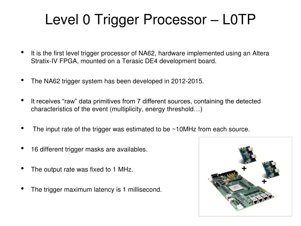
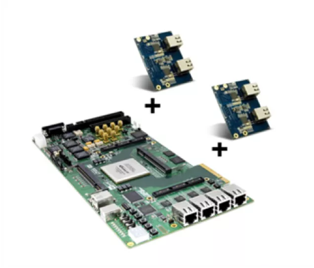
It is the first level trigger processor of NA62, hardware implemented using a
n Altera
Stratix
-IV
FPGA, mounted on a Terasic DE4
development
board.
•
The NA62 trigger system has been developed in 2012-2015.
•
It receives “raw” data primitives from 7 different sources, containing the detected
characteristics of the event (multiplicity, energy
threshold
…)
•
The input rate of the trigger was estimated to be ~10MHz from each source.
•
16 different trigger masks are availables.
•
The output rate was fixed to 1 MHz.
•
The trigger maximum latency is 1 millisecond.

A new L0TP system:
t
he L0TP+
•
An upgrade
of the
trigger processor is needed to run safely at the NA62 full intensity.
•
The NA62 Collaboration has initiated a feasibility study to establish how a
substantially better precision could be reached in a data taking at higher beam
intensity after Long Shutdown 3, going above the 100%.
•
The L0TP+ is based on a new platform
(the Xilinx VCU118 development board) that
can
implement
a faster and optimised firmware for higher
bandwidth primitive streams,
it will:
- replace the current L0TP without affecting the interfaced systems;
-
feature more trigger masks and smarter decision criteria, optimising the data
taking;
- add new functionalities, e.g. a PCI Express interface (see next slides);
- avoid potential obsolescence issues of current 2012 Altera Stratix-IV based
platform.
L0TP
I
nputs
•
The input rate reaches ~17MHz at 85% of the nominal intensity.
•
The L0TP system is able to run up to 25MHz of input rate, using a 1Gbit ethernet connection.
•
Nevertheless the experience showed big fluctuations of the beam instantaneous frequency.
•
The new L0TP+
can implement
10Gbit connections, cancelling any issue due to the rate, even
in the hypothesis of running at > 100%.
3
0
%
a
b
o
v
e
t
h
e
a
v
e
r
a
g
e
i
n
t
e
n
s
i
t
y
physics triggers Vs control triggers
•
The
current
L0TP-FPGA is limited in memory: primitives have to be re-aligned in time before
doing any coincidence searching, and this require big buffers addressed by the primitive time.
•
L0TP cannot read all the memory locations in time with
the
latency
.
•
A detector is “elected” as reference, and the memory locations containing this detector are
read: it has to be always in the trigger (defined as physics trigger).
•
To estimate the trigger efficiencies and to have an independent trigger stream, a control trigger
flux is implemented, which reads the non-empty addresses of a second primitive-source.
•
This baroque logic can be simplified having more
resources
(in particular on-chip memory)
on
the FPGA device
, as in the
Xilinx Virtex Ultrascale+ VU9P of the selected development board
.
•
For each trigger, the L0TP sends all the informations used to generate a trigger to
the PC-farm
using a dedicated 1GbE connection.
•
1 MHz is an intrinsic limit of the L0TP, due to the data format size.
•
L0TP+
can use
a
10
Gigabit ethernet
connection to the PC-farm
to overcome this
limitation (25/100 GbE channels are also available for other purposes).
O
utputs
•
NA62 collects all the input trigger primitives every 10 bursts, in order to check the trigger
performances and monitor the beam.
•
A series of switches are connected to the primitive stream in order to dump them in a PC.
•
The new L0TP+
can
dumps the primitives into
the host PC memory directly
via
a
PCI
Express
interface.
Additional Features of
L0TP+
The L0TP+ Platform: Xilinx VCU118 Dev Board
The Xilinx VCU118 platform is a major technological upgrade respect to
the Altera DE-4 both in terms of HW capabilities and development tools:
Virtex Ultrascale+ VU9P FPGA
C/C++
R
T
L
V
e
r
i
f
i
c
a
t
i
o
n
HLS Tools
RTL
F
u
n
c
t
i
o
n
a
l
V
e
r
i
f
i
c
a
t
i
o
n
w
i
t
h
C
/
C
+
+
c
o
m
p
i
l
e
r
Total available network bandwidth:
36x28 Gbps =
1 Tbps
Many configurations are possible using 1/10/28/40/100 GbE channels, even GBT channels…
Memory & Processing
•
345.9 Mbit
on-chip SRAM
•
Peak INT8 DSP:
21.3 TOP/s
Funding Requests
•
Need to procure the hardware for two complete L0TP+ systems:
•
Cost of off-the-shelf component for a single system: 11.500
€
.
•
Cost of the design of a FMC daughtercard to interface with the auxiliary board (Clock,
Burst and Choke/Error signals), and production of a small batch (5): 5.000
€
.
•
Total funding requests: 28.000
€
(vat included).
L0TP+ Development, Test and Deployment
•
Releases
•
Oct 19 Platform validation (physical interfaces & protocols,…)
•
1Q/2Q 20 First release with current L0TP functionalities.
•
4Q 20 Second release with PCI Express capabilities.
•
2Q 21 Third release ready for data taking.
•
Test activities
•
Testbench platform (Stratix IV based) in development sites for continuous no-
regression tests. Primitives pre-loaded in memory and sent through 4 GbE links to
L0TP+ to emulate TEL62s.
•
Pisa «realistic» Testbed (n TEL62, m PATTI, LTU) for validation of major releases.
Primitives can be generated by PATTI or loaded from memory.
Fundamental to test the synchronous behaviour and the full set of signals, trying to
reproduce the spiky timing behaviour of the beam.
•
Deployment
•
2021 parasitic test: test the L0TP+ in parallel with the current L0TP in order to
compare the performances and test new firmware solutions.
•
2022: switch between L0TP and L0TP+.
NA62 utilizes a Level 0 Trigger Processor (L0TP) for data processing. A new L0TP+ system, based on Xilinx VCU118, is being developed to improve precision, bandwidth, and functionality. It will optimize trigger masks, decision criteria, and address memory limitations.

Download Presentation

Please find below an Image/Link to download the presentation.
The content on the website is provided AS IS for your information and personal use only. It may not be sold, licensed, or shared on other websites without obtaining consent from the author.If you encounter any issues during the download, it is possible that the publisher has removed the file from their server.
You are allowed to download the files provided on this website for personal or commercial use, subject to the condition that they are used lawfully. All files are the property of their respective owners.
The content on the website is provided AS IS for your information and personal use only. It may not be sold, licensed, or shared on other websites without obtaining consent from the author.
E N D
Presentation Transcript
Level 0 Trigger Processor L0TP It is the first level trigger processor of NA62, hardware implemented using an Altera Stratix-IV FPGA, mounted on a Terasic DE4 development board. The NA62 trigger system has been developed in 2012-2015. It receives raw data primitives from 7 different sources, containing the detected characteristics of the event (multiplicity, energy threshold ) The input rate of the trigger was estimated to be ~10MHz from each source. 16 different trigger masks are availables. The output rate was fixed to 1 MHz. The trigger maximum latency is 1 millisecond.
A new L0TP system: the L0TP+ An upgrade of the trigger processor is needed to run safely at the NA62 full intensity. The NA62 Collaboration has initiated a feasibility study to establish how a substantially better precision could be reached in a data taking at higher beam intensity after Long Shutdown 3, going above the 100%. The L0TP+ is based on a new platform (the Xilinx VCU118 development board) that can implement a faster and optimised firmware for higher bandwidth primitive streams, it will: - replace the current L0TP without affecting the interfaced systems; - feature more trigger masks and smarter decision criteria, optimising the data taking; - add new functionalities, e.g. a PCI Express interface (see next slides); - avoid potential obsolescence issues of current 2012 Altera Stratix-IV based platform.
L0TP Inputs 30% above the average intensity The input rate reaches ~17MHz at 85% of the nominal intensity. The L0TP system is able to run up to 25MHz of input rate, using a 1Gbit ethernet connection. Nevertheless the experience showed big fluctuations of the beam instantaneous frequency. The new L0TP+ can implement 10Gbit connections, cancelling any issue due to the rate, even in the hypothesis of running at > 100%.
physics triggers Vs control triggers The current L0TP-FPGA is limited in memory: primitives have to be re-aligned in time before doing any coincidence searching, and this require big buffers addressed by the primitive time. L0TP cannot read all the memory locations in time with the latency. A detector is elected as reference, and the memory locations containing this detector are read: it has to be always in the trigger (defined as physics trigger). To estimate the trigger efficiencies and to have an independent trigger stream, a control trigger flux is implemented, which reads the non-empty addresses of a second primitive-source. This baroque logic can be simplified having more resources (in particular on-chip memory) on the FPGA device, as in the Xilinx Virtex Ultrascale+ VU9P of the selected development board.
Outputs For each trigger, the L0TP sends all the informations used to generate a trigger to the PC-farm using a dedicated 1GbE connection. 1 MHz is an intrinsic limit of the L0TP, due to the data format size. L0TP+ can use a 10 Gigabit ethernet connection to the PC-farm to overcome this limitation (25/100 GbE channels are also available for other purposes).
Additional Features of L0TP+ NA62 collects all the input trigger primitives every 10 bursts, in order to check the trigger performances and monitor the beam. A series of switches are connected to the primitive stream in order to dump them in a PC. The new L0TP+ can dumps the primitives into the host PC memory directly via a PCI Express interface.
The L0TP+ Platform: Xilinx VCU118 Dev Board The Xilinx VCU118 platform is a major technological upgrade respect to the Altera DE-4 both in terms of HW capabilities and development tools: Virtex Ultrascale+ VU9P FPGA Functional Verification with C/C++ compiler C/C++ HLS Tools RTL RTL Verification Total available network bandwidth: 36x28 Gbps = 1 Tbps Many configurations are possible using 1/10/28/40/100 GbE channels, even GBT channels Memory & Processing 345.9 Mbit on-chip SRAM Peak INT8 DSP: 21.3 TOP/s
Funding Requests Need to procure the hardware for two complete L0TP+ systems: Cost of off-the-shelf component for a single system: 11.500 . Cost of the design of a FMC daughtercard to interface with the auxiliary board (Clock, Burst and Choke/Error signals), and production of a small batch (5): 5.000 . Total funding requests: 28.000 (vat included). Splitter Module FMC+ (Vita57.4) to x2 FMC (Vita57.1) Component Unitary Cost Numerosity Cost Free FMC slot Xilinx VCU118 Dev Board 1 7310 7310 10-Port SFP+ (10G) FMC Module (Vita57.1) FMC+ to x2 FMC Splitter Module 1 1170 1170 10-Port SFP+ (10G) FMC Module 1 1650 1650 FMC Card Interface to Auxiliary Board (TTC& Choke/Err) FMC+ Extender Cable 1 1115 1115 1/10GbE SFP+ port (RJ45) SFP RJ45 Transc. Mod., 1000Base-T 8 30 240
L0TP+ Development, Test and Deployment Releases Oct 19 Platform validation (physical interfaces & protocols, ) 1Q/2Q 20 First release with current L0TP functionalities. 4Q 20 Second release with PCI Express capabilities. 2Q 21 Third release ready for data taking. Test activities Testbench platform (Stratix IV based) in development sites for continuous no- regression tests. Primitives pre-loaded in memory and sent through 4 GbE links to L0TP+ to emulate TEL62s. Pisa realistic Testbed (n TEL62, m PATTI, LTU) for validation of major releases. Primitives can be generated by PATTI or loaded from memory. Fundamental to test the synchronous behaviour and the full set of signals, trying to reproduce the spiky timing behaviour of the beam. Deployment 2021 parasitic test: test the L0TP+ in parallel with the current L0TP in order to compare the performances and test new firmware solutions. 2022: switch between L0TP and L0TP+.