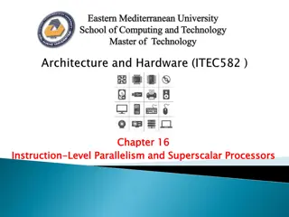
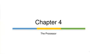
Development of Multiclock Cycle in Processor
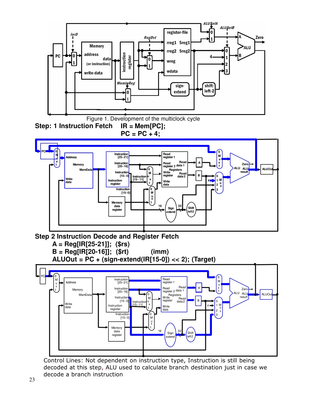

Figure
1.
Development
of the multiclock
cycle
S
t
e
p
:
1
I
n
s
t
r
u
c
t
i
o
n
F
e
t
c
h
I
R
=
M
e
m
[
P
C
]
;
P
C
=
P
C
+
4
;
S
t
e
p
2
I
n
s
t
r
u
c
t
i
o
n
D
e
c
o
d
e
a
n
d
R
e
g
i
s
t
e
r
F
e
t
c
h
A
=
R
e
g
[
I
R
[
2
5
-
2
1
]
]
;
(
$
r
s
)
B
=
R
e
g
[
I
R
[
2
0
-
1
6
]
]
;
(
$
r
t
)
(
i
m
m
)
A
L
U
O
u
t
=
P
C
+
(
s
i
g
n
-
e
x
t
e
n
d
(
I
R
[
1
5
-
0
]
)
<
<
2
)
;
(
T
a
r
g
e
t
)
Control Lines: Not
dependent
on
instruction
type,
Instruction
is still
being
decoded
at
this
step
,
ALU used
to
calculate
branch
destination just in case
we
decode a branch
instruction

S
h
i
f
t
left
2

PC

Memory
M
e
m
D
a
t
a
W
r
i
t
e
data

0
M
u
x
1

register
W
r
i
t
e
data
R
e
a
d
R
e
a
d
data
2
Read
register
1
R
ead
register
2
data
1
Registers
Write

M
x
0
1

0
M
u
x
1

4

I
n
s
t
ru
c
t
i
o
n
[
1
5
–
0
]
Sign
e
x
t
end
32

16

In
st
r
u
c
t
i
o
n
[25–
21]
In
st
r
u
c
t
i
o
n
[20–
16]

In
st
r
u
c
t
i
o
n
[1
5
–
0
]
Instruction
register
x
0
1
M
3
u
2

Z
e
r
o
ALU
ALU
result

M
e
m
o
r
y
data
register

Instruction
u
[15–
11]


A
B

ALUOut

0
M
u
x
1
A
ddress

S
h
i
f
t
l
e
f
t
2

M
u
x

P
C
0
1

r
e
g
i
s
t
e
r
W
r
i
t
e
d
a
t
a
R
e
a
d
R
e
a
d
d
a
t
a
2
R
e
a
d
r
e
g
i
s
t
e
r
1
R
e
a
d
r
e
g
i
s
t
e
r
2
d
a
t
a
1
R
e
g
i
s
t
e
r
s
W
r
i
t
e

M
0

0
M
u
x
1

4

I
n
s
t
r
u
c
t
i
o
n
[
1
5
–
0
]
S
i
g
n
e
x
t
e
n
d
3
2

1
6

I
n
s
t
r
u
c
t
i
o
n
[
2
5
–
2
1
]
I
n
s
t
r
u
c
t
i
o
n
[
2
0
–
1
6
]

I
n
s
t
r
u
c
t
i
o
n
[
1
5
–
0
]
I
n
s
t
r
u
c
t
i
o
n
r
e
g
i
s
t
e
r
1
M
x
0
3
2
u

A
L
U
A
L
U
r
e
s
u
l
t

Z
e
r
o

M
e
m
o
r
y
d
a
t
a
r
e
g
i
s
t
e
r

I
n
s
t
r
u
c
t
i
o
n
u
[
1
5
–
1
1
]
x
1


A
B

A
L
U
O
u
t

0
M
u
x
1

A
d
d
r
e
s
s
M
e
m
o
r
y
M
e
m
D
a
t
a
W
r
i
t
e
d
a
t
a


23

S
t
e
p
3
R
-
T
y
p
e
E
x
e
c
u
t
i
o
n
A
L
U
O
u
t
=
A
o
p
B
;
S
t
e
p
4
R
-
T
y
p
e
W
r
i
t
e
B
a
c
k
R
e
g
[
I
R
[
1
5
-
1
1
]
]
=
A
L
U
O
u
t
;
(
$
r
d
A
L
U
O
u
t
)
This is
the
last
step for
R-Type
S
t
e
p
3
:
B
r
a
n
c
h
E
x
e
c
u
t
i
o
n
i
f
(
A
=
=
B
)
P
C
=
A
L
U
O
u
t
(
t
a
r
g
e
t
)
This is
the
last
step for
Branch

S
h
i
f
t
left
2

M
u
x

PC
0
1

R
e
g
i
s
t
e
rs
Write
register
W
r
i
t
e
data
R
e
a
d
R
e
a
d
data
2
Read
register
1
Read
register
2
data
1

M
0
1

0
M
u
x
1

4

I
n
s
t
r
u
c
t
ion
[
1
5
–
0
]
Sign
e
x
t
e
n
d
32

16

In
s
t
r
u
c
t
i
o
n
[25–
21]
In
s
t
r
u
c
t
i
o
n
[20–
16]

In
s
t
r
u
c
t
i
o
n
[
1
5
–
0]
Instruction
r
e
g
i
s
t
e
r
x
0
1
M
3
u
2

ALU
ALU
result

Z
e
r
o

M
e
m
o
r
y
data
r
e
gis
te
r

Instruction
u
[15–
11]
x


A
B

A
L
UO
ut

0
M
u
x
1

Address
Memory
M
em
Dat
a
W
r
i
t
e
data


S
h
i
f
t
left
2

M
u
x

P
C
0
1

R
e
g
is
t
e
r
s
Write
r
e
g
i
s
t
e
r
Wr
ite
data
R
e
a
d
R
e
a
d
data
2
Read
register
1
Read
register
2
data
1

M
0
x
1

0
M
u
x
1

4

I
n
s
tr
u
c
t
i
o
n
[
1
5
–
0
]
Sign
e
x
tend
32

16

Instruction
[
2
5
–
2
1
]
Instruction
[
2
0
–
1
6
]

I
n
s
t
r
u
c
t
i
o
n
[15
–
0
]
In
s
t
r
u
c
t
i
o
n
register
x
0
1
M
3
u
2

result
ALU
ALU

Z
e
ro

M
e
m
o
r
y
data
r
e
g
i
s
te
r

Instruction
u
[15–
11]


A
B

ALUOut

0
M
u
x
1

Address
Memory
M
e
m
D
a
t
a
W
r
i
t
e
data

S
h
i
f
t
left
2

M
u
x

P
C
0
1

register
W
r
i
t
e
data
R
e
a
d
R
e
a
d
data
2
Read
register
1
R
e
a
d
register
2
data
1
Registers
Write

M
0
1

0
M
u
x
1

4

I
n
s
t
ru
c
t
i
o
n
[1
5
–
0
]
Sign
e
x
t
end
32

16

I
n
st
r
u
c
t
i
o
n
[25–
21]
I
n
st
r
u
c
t
i
o
n
[20–
16]

I
n
st
r
u
c
t
i
o
n
[15–
0]
Instruction
register
x
0
1
M
3
2
u

ALU
ALU
result

Z
e
ro

M
e
m
o
r
y
data
r
e
g
is
t
er

Instruction
u
[15–
11]
x


A
B

A
L
U
O
u
t

0
M
u
x
1

Address
Memory
M
e
m
D
a
t
a
Wr
i
t
e
data

24
Step 3:
Memory
Execution
A
L
U
O
u
t
=
A
+
s
i
g
n
-
e
x
t
e
n
d
(
I
R
[
1
5
-
0
]
)
;
S
t
e
p
4
:
L
o
a
d
M
e
m
o
r
y
M
D
R
=
M
e
m
o
r
y
[
A
L
U
O
u
t
]
;
S
t
e
p
4
:
S
t
o
r
e
W
r
i
t
e
B
a
c
k
M
e
m
o
r
y
[
A
L
U
o
u
t
]
=
B
;
This
is
the last
step for
Store
S
h
i
f
t
left
2
M
u
x
P
C
0
1
R
e
g
i
s
t
e
r
s
Write
register
Wr
i
t
e
data
R
e
a
d
R
e
a
d
data
2
Read
register
1
Read
register
2
data
1
M
0
x
1
M
u
0
x
1
4
I
ns
t
r
u
c
t
i
o
n
[
1
5
–
0
]
Sign
e
xt
end
32
16
I
n
s
t
r
u
cti
o
n
[
2
5
–
2
1
]
I
n
s
t
r
u
cti
o
n
[
2
0
–
1
6
]
I
n
s
t
r
u
cti
o
n
[
15
–
0
]
I
n
s
t
ru
c
t
i
o
n
register
x
0
1
M
3
u
2
r
e
s
u
l
t
ALU
ALU
Z
e
ro
M
e
m
o
r
y
data
r
e
gi
s
t
e
r
Instruction
u
[15–
11]
A
B
ALUOut
0
M
u
x
1
Address
Memory
M
e
m
D
a
t
a
W
r
i
t
e
data
S
h
i
f
t
left
2
M
u
x
P
C
0
1
register
W
r
it
e
data
R
e
a
d
R
e
a
d
data
2
Read
register
1
R
e
a
d
register
2
data
1
Registers
Write
M
0
1
0
M
u
x
1
4
I
n
s
tr
u
c
t
i
o
n
[
1
5
–
0
]
Sign
e
x
t
e
n
d
32
16
In
s
t
r
u
ct
i
o
n
[25–
21]
In
s
t
r
u
ct
i
o
n
[20–
16]
In
s
t
r
u
ct
i
o
n
[15–
0]
Instruction
register
x
0
1
M
3
u
2
ALU
ALU
result
Z
e
r
o
M
e
m
o
r
y
data
re
g
i
s
ter
Instruction
u
[15–
11]
x
A
B
AL
U
O
u
t
0
M
u
x
1
Address
Memory
M
e
mD
a
t
a
W
r
i
t
e
data
S
h
i
f
t
left
2
M
u
x
P
C
0
1
register
W
r
it
e
data
R
e
a
d
R
e
a
d
data
2
Read
register
1
R
e
a
d
register
2
data
1
Registers
Write
M
0
M
u
0
x
1
4
I
n
s
tr
u
c
t
i
o
n
[15–
0]
S
i
g
n
e
x
t
e
n
d
32
16
In
s
t
r
u
ct
i
o
n
[25–
21]
In
s
t
r
u
ct
i
o
n
[20–
16]
In
s
t
r
u
ct
i
o
n
[15–
0]
I
n
s
t
ru
c
t
i
on
register
x
0
1
M
3
u
2
r
e
s
u
l
t
ALU
ALU
Z
e
r
o
M
e
m
o
r
y
data
re
g
i
s
ter
Instruction
u
[
1
5
–
11
]
x
1
A
B
AL
U
O
u
t
0
M
u
x
1
Address
Memory
M
e
mD
a
t
a
W
r
i
t
e
data
25
S
t
e
p
5
:
L
o
a
d
W
r
i
t
e
B
a
c
k
R
e
g
[
I
R
[
2
0
-
1
6
]
]
=
M
D
R
;
This
is
the last step
for
Load
S
h
i
f
t
left
2
M
u
x
P
C
0
1
register
W
r
it
e
data
R
e
a
d
R
e
a
d
data
2
Read
register
1
R
e
a
d
register
2
data
1
Registers
Write
M
0
x
1
M
u
0
x
1
4
I
n
s
tr
u
c
t
i
o
n
[
1
5
–
0
]
Sign
e
x
t
e
n
d
32
16
In
s
t
r
u
ct
i
o
n
[25–
21]
In
s
t
r
u
ct
i
o
n
[20–
16]
In
s
t
r
u
ct
i
o
n
[15–
0]
I
n
s
t
ru
c
t
i
on
register
x
0
1
M
3
u
2
r
e
s
u
l
t
ALU
ALU
Z
e
r
o
M
e
m
o
r
y
data
re
g
i
s
ter
Instruction
u
[15–
11]
A
B
AL
U
O
u
t
0
M
u
x
1
Address
Memory
M
e
mD
a
t
a
W
r
i
t
e
data
1
;
1
;
1
;
00;
1
;
27
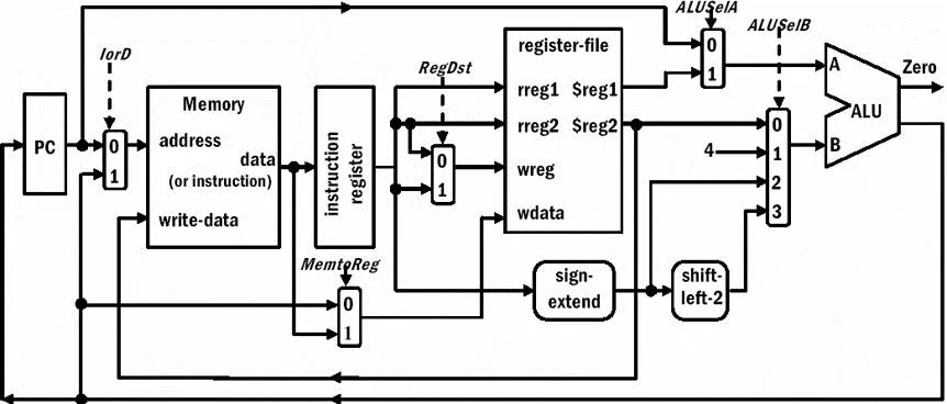
The development process of the multiclock cycle in a processor is explained in detail through different steps, including instruction fetch, decode, register fetch, execution, and write-back for R-type instructions. Control lines and branching execution are also covered in the description. The content provides insights into the intricate workings of processor cycles and highlights key operations involved at each stage.

Download Presentation

Please find below an Image/Link to download the presentation.
The content on the website is provided AS IS for your information and personal use only. It may not be sold, licensed, or shared on other websites without obtaining consent from the author.If you encounter any issues during the download, it is possible that the publisher has removed the file from their server.
You are allowed to download the files provided on this website for personal or commercial use, subject to the condition that they are used lawfully. All files are the property of their respective owners.
The content on the website is provided AS IS for your information and personal use only. It may not be sold, licensed, or shared on other websites without obtaining consent from the author.
E N D
Presentation Transcript
Figure 1. Development of the multiclock cycle Step: 1 Instruction Fetch IR = Mem[PC]; PC = PC + 4; PC 0 0 M u x 1 Instruction [25 21] Read register1 M u x 1 Address Read A Instruction [20 16] Read register 2 data 1 Registers Write Zero Memory ALU ALU result ALUOut 0 MemData Instruction [15 0] Instruction register M Read data2 register B 0 Instructionu [15 11] Write data x 1M 2u 4 Write data 1 x 0 M u x 1 Instruction [15 0] 3 Memory data register 16 32 Shift left2 Sign extend Step 2 Instruction Decode and Register Fetch A = Reg[IR[25-21]]; ($rs) B = Reg[IR[20-16]]; ($rt) ALUOut = PC + (sign-extend(IR[15-0]) << 2); (Target) (imm) PC 0 M u x 1 0 M u x 1 Read register1 Instruction [25 21] Address Read A Read register 2 data 1 Registers Write Instruction [20 16] Zero Memory ALU ALU result 0 ALUOut MemData Instruction [15 0] Instruction register M Read data2 register B Instructionu [15 11] 0 1 M Write data x 4 Write data u 1 2 x Instruction [15 0] 0 M u x 1 3 Memory data register 16 32 Shift left2 Sign extend Control Lines: Not dependent on instruction type, Instruction is still being decoded at this step, ALU used to calculate branch destination just in case we decode a branch instruction 23
Step 3 R-Type Execution ALUOut = A op B; PC 0 0 M u x 1 Instruction [25 21] Read register1 M u x 1 Address Read A Read register 2 data 1 Registers Write Instruction [20 16] Zero Memory ALUALU result ALUOut 0 MemData Instruction [15 0] Instruction register M Read data2 register B 0 1M 2u Instruction u [15 11] Write data x 4 Write data 1 x Instruction [15 0] 0 M u x 1 3 Memory data register 16 32 Shift left2 Sign extend Step 4 R-Type Write Back Reg[IR[15-11]] = ALUOut; ($rd ALUOut) This is the last step for R-Type PC 0 0 M u x 1 Instruction [25 21] Read register1 M u x 1 Address Read A Read register 2 data1 Instruction [20 16] Zero Memory ALUALU ALUOut 0 MemData Registers Write register result Instruction [15 0] M Read data2 B Instructionu [15 11] 0 1M 2 x 1 Write data 4 Instruction register Write data u x 0 M u x 1 Instruction [15 0] 3 Memory data register 16 32 Shift left2 Sign extend Step 3: Branch Execution if (A == B) PC = ALUOut (target) This is the last step for Branch PC 0 0 M u x 1 Instruction [25 21] Read register1 M u x 1 Address Read A Read register 2 data1 Instruction [20 16] Zero Memory ALUALU result ALUOut 0 MemData Registers Write register Instruction [15 0] M Read data2 B 0 1M 2 Instruction u [15 11] Write data x 4 Instruction register Write data u 1 x Instruction [15 0] 0 M u x 1 3 Memory data register 16 32 Sign extend Shift left2 24
Step 3: Memory Execution ALUOut = A + sign-extend(IR[15-0]); PC 0 0 M u x 1 Instruction [25 21] Read register1 M u x 1 Address Read A Instruction [20 16] Read register 2 data 1 Registers Write Zero Memory ALU ALU result ALUOut 0 MemData Instruction [15 0] Instruction register M Read data2 register B 0 1M 2 Instruction u [15 11] Write data x 4 Write data u 1 x Instruction [15 0] 0 M u x 1 3 Memory data register 16 32 Shift left2 Sign extend Step 4: Load Memory MDR = Memory[ALUOut]; PC 0 0 M u x 1 Instruction [25 21] Read register1 M u x 1 Address Read A Read register 2 data1 Instruction [20 16] Zero Memory ALUALU ALUOut 0 MemData Registers Write register result Instruction [15 0] M Read data2 B 0 1 M 2 Instruction u [15 11] x 1 Write data 4 Instruction register Write data u x Instruction [15 0] 0 3 M u x 1 Memory data register 16 32 Sign extend Shift left2 Step 4: Store Write Back Memory[ALUout] = B; This is the last step for Store PC 0 0 M u x 1 Instruction [25 21] Read register1 M u x 1 Address Read A Read register 2 data 1 Registers Write Instruction [20 16] Zero Memory ALU ALU ALUOut 0 MemData result Instruction [15 0] M Read data2 register B 0 1M 2 Instruction u [15 11] x Write data 4 Instruction register Write data u 1 x 0 Instruction [15 0] 3 M u x 1 Memory data register 16 32 Shift left2 Sign extend 25
Step 5: Load Write Back Reg[IR[20-16]] = MDR; This is the last step for Load PC 0 0 M u x 1 Instruction [25 21] Read register1 M u x 1 Address Read A Read register 2 data 1 Registers Write Instruction [20 16] Zero Memory ALU ALU ALUOut 0 MemData result Instruction [15 0] M Read data2 register B 0 1M 2 Instruction u [15 11] Write data x 1 4 Instruction register Write data u x Instruction [15 0] 0 3 M u x 1 Memory data register 16 32 Shift left2 Sign extend
1; 1; 1; 00; 1; 27