DEQ BMP Warehouse

Conductors, Insulators, and
Semiconductors
nano@Illinois RET module
C. Britt Carlson, PhD
Parkland College

B
a
n
d
T
h
e
o
r
y
o
f
C
o
n
d
u
c
t
i
v
i
t
y
2
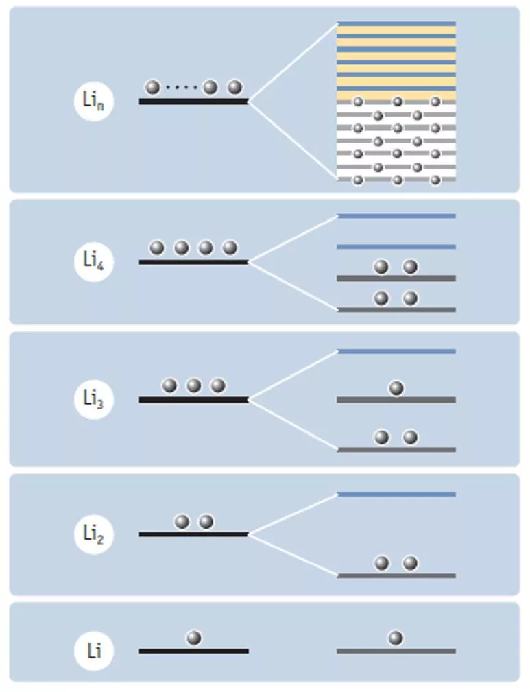
The basis for the difference of conductivity
of elements can be considered in terms
of how the electrons are organized in a
pure solid sample of the element.
In solids, atoms are closely packed, leading
to overlapping molecular orbitals and
bands of electrons.
These large overlapping molecular orbitals
create bands, a valence band and a
higher energy conduction band.
The energy difference between these two
bands is known as the band gap energy.
(Burdge and Overby 914-915, Kotz,
Treichel, and Townsend 595-598).
(Kotz, Treichel, and Townsend 597)
B
B
a
a
n
n
d
d
T
T
h
h
e
e
o
o
r
r
y
y
o
o
f
f
C
C
o
o
n
n
d
d
u
u
c
c
t
t
i
i
v
v
i
i
t
t
y
y
3
•
When there is a very small band gap energy, electrons can easily jump into
the conduction band, where they are more delocalized and can move more
freely. This allows the electrical current to be conducted across the sample
(Burdge and Overby 914-915).
•
This explains one of the major difference between conductors, semi-
conductors, and insulators. Conducting materials have a small band gap
energy, insulators have a large band gap energy, and semiconductors are in
between
(Burdge and Overby 914-915).
(Burdge and Overby 1021)
B
a
n
d
T
h
e
o
r
y
o
f
C
o
n
d
u
c
t
i
v
i
t
y
4
“The ability of a semiconductor to conduct electricity can be enhanced by
adding small amounts of impurities to the element, a process called
doping
”
(Burdge and Overby 914-915).
S
o
l
i
d
s
c
o
n
t
a
i
n
i
n
g
e
l
e
c
t
r
o
n
d
o
n
o
r
i
m
p
u
r
i
t
i
e
s
a
r
e
c
a
l
l
e
d
n
-
t
y
p
e
s
e
m
i
c
o
n
d
u
c
t
o
r
s
.
S
e
m
i
c
o
n
d
u
c
t
o
r
s
t
h
a
t
c
o
n
t
a
i
n
a
c
c
e
p
t
o
r
i
m
p
u
r
i
t
i
e
s
a
r
e
c
a
l
l
e
d
p
-
t
y
p
e
s
e
m
i
c
o
n
d
u
c
t
o
r
s
(
B
u
r
d
g
e
a
n
d
O
v
e
r
b
y
9
1
4
-
9
1
5
)
.
(Burdge and Overby 915)
•
C
h
o
o
s
e
o
n
e
:
A
S
i
s
a
m
p
l
e
d
o
p
e
d
w
i
t
h
b
o
r
o
n
i
s
(
n
-
t
y
p
e
o
r
p
-
t
y
p
e
)
?
•
C
h
o
o
s
e
o
n
e
:
A
S
i
s
a
m
p
l
e
d
o
p
e
d
w
i
t
h
a
n
t
i
m
o
n
y
i
s
(
n
-
t
y
p
e
o
r
p
-
t
y
p
e
)
?
5
S
S
e
e
m
m
i
i
-
-
c
c
o
o
n
n
d
d
u
u
c
c
t
t
o
o
r
r
p
p
r
r
a
a
c
c
t
t
i
i
c
c
e
e
Answer: p-type
Answer: n-type
Look at the image.
1. Is this n-type or p-type doping?
2. What is the dopant?
3. What does “n-” vs “p-” mean?
4. What would the other type look like?
6
http://demonstrations.wolfram.com/DopedSiliconSemiconductors/
Answers:
1. n-type
2. P
3. Definitions are on slide 4
4. See slide 7
P-type example
7
B only has 3
valence electrons
compared to Si’s 4
valence electron.
This absence of a
4
th
electron is called
a “hole.”
Blinder, S. M.
This is p-type doping of silicon, where B is the dopant.
S
e
m
i
c
o
n
d
u
c
t
o
r
s
8
•
A Schottky barrier is a potential energy barrier for electrons formed at a metal-
semiconductor junction.
•
Depending on the doping type (n-type versus p-type) and the doping level
(density of doping atoms) of the semiconductor and the electronic properties of
the metal, a Schottky barrier will form a diode.
•
A diode is an electronic circuit element that primarily flows current in only one
direction and blocks current from flowing in the opposite direction.
•
Directing the flow of current has many different uses, including when generating
light in light-emitting diodes (LEDs) (Kotz, Treichel, and Townsend 598).
The Experiment
•
Make circuits with various electrodes and a variable voltage source.
•
Safety issues:
•
To reduce the chance of accident shocks, make sure that the electrodes
never touch and that the alligator clips for each electrode don’t touch until
you are ready.
•
Keep the energy source turned off until just before you test the electrodes.
•
Do not exceed 10V.
•
Make sure to handle glass, metal, and silicon wafers with caution – the
edges can be sharp.
•
Disconnect any circuit that feels like it is starting to get hot.
Part I: Experimental Set-up
Basic schematic of the circuit.
Yellow: the energy source, Grey:
the multimeter, Black: the wires,
Orange: the electrodes.
Image edited from:
http://www.funsci.com/fun3_en/el
ectro/elec_02.gif
red
wire
red wire
black wire
#
2
#
1
⊕
⊝
Part II: Circuit with known electrodes
•
Set the power source to 1V (
record the exact setting
), connect the metal
sample as the 2
nd
electrode and use the multimeter to determine the
amperage.
It should read 0 if the electrodes are still not touching.
•
Carefully touch the two metal electrodes to each other.
Make sure to
record the voltage and amperage numbers and also observations.
•
If multimeter doesn’t show an amperage reading, separate the
electrodes, change the power source to 2V and then try again. Continue
slowly testing increases in voltage (1 V at a time) until you get to a
maximum of 10V.
•
Repeat this procedure for all the following:
•
The glass coverslip
•
Each of the silicon wafers (1 undoped sample, 1 highly doped sample,
2 medium doped samples (1
p
-type and 1
n
-type)).
•
Note: you will need to change the metal to the black wire and the
n-
type
silicon to the red wire when you do this sample.
Part III: Circuit with unknown electrode
•
Connect the first unknown sample as the 2
nd
electrode and use the
multimeter to determine the amperage of the circuit.
Make sure to record
the numbers and also observations.
•
Using the voltage and amperage data, determine if your unknown is a
conductor, insulator or semiconductor.
•
If your sample is a semiconductor, determine if it has
•
high or low doping
•
p-
type or
n-
type doping
F
i
n
i
s
h
i
n
g
t
h
e
l
a
b
r
e
p
o
r
t
•
Answer the lab questions and complete the lab report, according to the
Anatomy of a Lab Report or other format, as applicable.
R
e
f
e
r
e
n
c
e
s
•
Burdge, Julia R., and Jason Overby. Chemistry: Atoms First. 2nd ed.
New York, NY: McGraw-Hill Education, 2015. Print.
•
Kotz, John C., Treichel, Paul M., and John R. Townsend. Chemistry and
Chemical Reactivity. 8
th
ed. Belmont, CA: Cengage Learning, 2012.
Print.
•
Blinder, S. M. "Doped Silicon Semiconductors."
Wolfram
Demonstrations Project
. Wolfram Demonstrations Project &
Contributors, n.d. Web. 24 Mar. 2016.
<http://demonstrations.wolfram.com/DopedSiliconSemiconductors/>
DEQ BMP Warehouse is a platform for reporting templates and scenarios related to Best Management Practices. It includes tools for urban-suburban, agricultural, and grant reporting, detailing BMPs to be reported and those exempt from reporting.

Download Presentation

Please find below an Image/Link to download the presentation.
The content on the website is provided AS IS for your information and personal use only. It may not be sold, licensed, or shared on other websites without obtaining consent from the author.If you encounter any issues during the download, it is possible that the publisher has removed the file from their server.
You are allowed to download the files provided on this website for personal or commercial use, subject to the condition that they are used lawfully. All files are the property of their respective owners.
The content on the website is provided AS IS for your information and personal use only. It may not be sold, licensed, or shared on other websites without obtaining consent from the author.
E N D
Presentation Transcript
Conductors, Insulators, and Semiconductors nano@Illinois RET module C. Britt Carlson, PhD Parkland College
Band Theory of Conductivity Band Theory of Conductivity The basis for the difference of conductivity of elements can be considered in terms of how the electrons are organized in a pure solid sample of the element. In solids, atoms are closely packed, leading to overlapping molecular orbitals and bands of electrons. These large overlapping molecular orbitals create bands, a valence band and a higher energy conduction band. The energy difference between these two bands is known as the band gap energy. (Burdge and Overby 914-915, Kotz, Treichel, and Townsend 595-598). 2 (Kotz, Treichel, and Townsend 597)
Band Theory of Band Theory of Conductivity When there is a very small band gap energy, electrons can easily jump into the conduction band, where they are more delocalized and can move more freely. This allows the electrical current to be conducted across the sample (Burdge and Overby 914-915). Conductivity (Burdge and Overby 1021) This explains one of the major difference between conductors, semi- conductors, and insulators. Conducting materials have a small band gap energy, insulators have a large band gap energy, and semiconductors are in between (Burdge and Overby 914-915). 3
Band Theory of Conductivity The ability of a semiconductor to conduct electricity can be enhanced by adding small amounts of impurities to the element, a process called doping (Burdge and Overby 914-915). (Burdge and Overby 915) Solids containing electron donor impurities are called n-type semiconductors. Semiconductors that contain acceptor impurities are called p-type semiconductors (Burdge and Overby 914-915). 4
Semi-conductor practice Choose one: A Si sample doped with boron is (n-type or p-type)? Answer: p-type Choose one: A Si sample doped with antimony is (n-type or p-type)? Answer: n-type 5
Look at the image. 1. Is this n-type or p-type doping? http://demonstrations.wolfram.com/DopedSiliconSemiconductors/ 2. What is the dopant? Answers: 1. n-type 2. P 3. Definitions are on slide 4 4. See slide 7 3. What does n- vs p- mean? 4. What would the other type look like? 6
P-type example B only has 3 valence electrons compared to Si s 4 valence electron. This absence of a 4th electron is called a hole. Blinder, S. M. This is p-type doping of silicon, where B is the dopant. 7
Semiconductors A Schottky barrier is a potential energy barrier for electrons formed at a metal- semiconductor junction. Depending on the doping type (n-type versus p-type) and the doping level (density of doping atoms) of the semiconductor and the electronic properties of the metal, a Schottky barrier will form a diode. A diode is an electronic circuit element that primarily flows current in only one direction and blocks current from flowing in the opposite direction. Directing the flow of current has many different uses, including when generating light in light-emitting diodes (LEDs) (Kotz, Treichel, and Townsend 598). 8
The Experiment Make circuits with various electrodes and a variable voltage source. Safety issues: To reduce the chance of accident shocks, make sure that the electrodes never touch and that the alligator clips for each electrode don t touch until you are ready. Keep the energy source turned off until just before you test the electrodes. Do not exceed 10V. Make sure to handle glass, metal, and silicon wafers with caution the edges can be sharp. Disconnect any circuit that feels like it is starting to get hot.
Part I: Experimental Set-up Basic schematic of the circuit. Yellow: the energy source, Grey: the multimeter, Black: the wires, Orange: the electrodes. red wire Image edited from: http://www.funsci.com/fun3_en/el ectro/elec_02.gif black wire red wire # 2 # 1
Part II: Circuit with known electrodes Set the power source to 1V (record the exact setting), connect the metal sample as the 2nd electrode and use the multimeter to determine the amperage. It should read 0 if the electrodes are still not touching. Carefully touch the two metal electrodes to each other. Make sure to record the voltage and amperage numbers and also observations. If multimeter doesn t show an amperage reading, separate the electrodes, change the power source to 2V and then try again. Continue slowly testing increases in voltage (1 V at a time) until you get to a maximum of 10V. Repeat this procedure for all the following: The glass coverslip Each of the silicon wafers (1 undoped sample, 1 highly doped sample, 2 medium doped samples (1 p-type and 1 n-type)). Note: you will need to change the metal to the black wire and the n-type silicon to the red wire when you do this sample.
Part III: Circuit with unknown electrode Connect the first unknown sample as the 2nd electrode and use the multimeter to determine the amperage of the circuit. Make sure to record the numbers and also observations. Using the voltage and amperage data, determine if your unknown is a conductor, insulator or semiconductor. If your sample is a semiconductor, determine if it has high or low doping p-type or n-type doping
Finishing the lab report Finishing the lab report Answer the lab questions and complete the lab report, according to the Anatomy of a Lab Report or other format, as applicable.
References Burdge, Julia R., and Jason Overby. Chemistry: Atoms First. 2nd ed. New York, NY: McGraw-Hill Education, 2015. Print. Kotz, John C., Treichel, Paul M., and John R. Townsend. Chemistry and Chemical Reactivity. 8th ed. Belmont, CA: Cengage Learning, 2012. Print. Blinder, S. M. "Doped Silicon Semiconductors." Wolfram Demonstrations Project. Wolfram Demonstrations Project & Contributors, n.d. Web. 24 Mar. 2016. <http://demonstrations.wolfram.com/DopedSiliconSemiconductors/>