Crystal Lattice Imperfections Overview
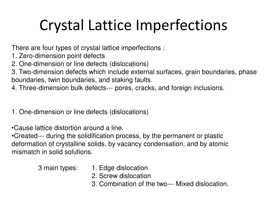

Crystal Lattice Imperfections
There are four types of crystal lattice imperfections :
1. Zero-dimension point defects
2. One-dimension or line defects (dislocations)
3. Two-dimension defects which include external surfaces, grain boundaries, phase
boundaries, twin boundaries, and staking faults.
4. Three-dimension bulk defects--- pores, cracks, and foreign inclusions.
1. One-dimension or line defects (dislocations)
•
Cause lattice distortion around a line.
•
Created--- during the solidification process, by the permanent or plastic
deformation of crystalline solids, by vacancy condensation, and by atomic
mismatch in solid solutions.
3 main types:
1. Edge dislocation
2. Screw dislocation
3. Combination of the two--- Mixed dislocation.
Edge Dislocation
1.
Extra half-plane of
atoms inserted in a
crystal structure.
2.
B
u
r
g
e
r
s
v
e
c
t
o
r
,
b
p
e
r
p
e
n
d
i
c
u
l
a
r
(
)
t
o
d
i
s
l
o
c
a
t
i
o
n
l
i
n
e
.
B
u
r
g
e
r
’
s
v
e
c
t
o
r
,
b
:
m
e
a
s
u
r
e
o
f
l
a
t
t
i
c
e
d
i
s
t
o
r
t
i
o
n
https://www.youtube.com/watch?v=-
t6btGjGKYU
3
Screw Dislocation
Screw Dislocation
The screw dislocation in (a) as viewed from above.
The dislocation line extends along line AB. Atom
positions above the slip plane are open circles and those
Below are solid circles.
Burgers vector
b
Dislocation
line
b
(a)
(b)
1.
spiral planar ramp resulting
from shear deformation.
2.
b
p
a
r
a
l
l
e
l
(
)
t
o
d
i
s
l
o
c
a
t
i
o
n
l
i
n
e
.
https://www.youtube.com/watch?v=TxJOP
3hA6To
4
Edge, Screw, and Mixed
Dislocations
Adapted from Fig. 4.5,
Callister & Rethwisch 8e.
5
Imperfections in Solids
Dislocations are visible in electron micrographs
Fig. 4.6,
Callister & Rethwisch 8e.
6
Grain Boundaries
•
regions between crystals
•
transition from lattice of
one region to that of the
other
•
slightly disordered
•
low density in grain
boundaries
–
high mobility
–
high diffusivity
–
high chemical reactivity
Adapted from Fig. 4.7,
Callister & Rethwisch 8e.
http://en.wikipedia.org/wiki/Grain_boundary
https://www.youtube.com/watch?v=uG35D_euM-0
TWIN BOUNDARIES
Twin boundary is a special type of grain boundary across which there is a specific
mirror lattice symmetry.
Two Types:
Mechanical twins: Result from atomic displacements that are produced from applied
mechanical shear forces. Found in BCC & HCP metals.
Annealing twins: Result during annealing heat treatments following deformation.
Found in FCC metals.
http://en.wikipedia.org/w
iki/Crystal_twinning
8
Microscopic Examination
•
Crystallites (grains) and grain boundaries vary
considerably in size. Can be quite large.
–
ex: Large single crystal of quartz or diamond or Si
–
ex: Aluminum light post or garbage can - see the
individual grains
•
Crystallites (grains) can be quite small (mm or
less) – necessary to observe with a microscope.
9
•Only the surface is observed, reflecting mode.
•
Useful up to 2000X magnification.
• Polishing removes surface features (e.g., scratches)
• Etching changes reflectance, depending on crystal
orientation.
Micrograph of
brass (a Cu-Zn alloy)
Optical Microscopy
Adapted from Fig. 4.13(b) and (c),
Callister &
Rethwisch 8e.
(Fig. 4.13(c) is courtesy
of J.E. Burke, General Electric Co.)
crystallographic planes
10
Grain boundaries...
• are imperfections,
• are more susceptible
to etching,
• may be revealed as
dark lines,
• change in crystal
orientation across
boundary.
Adapted from Fig. 4.14(a) and
(b),
Callister & Rethwisch 8e.
(Fig. 4.14(b) is courtesy
of L.C. Smith and C. Brady, the
National Bureau of Standards,
Washington, DC [now the
National Institute of Standards
and Technology, Gaithersburg,
MD].)
Optical Microscopy
11
Microscopy
Optical resolution: 10
-7
m = 0.1
m = 100 nm
For higher resolution need higher frequency
–
X-Rays? Difficult to focus.
–
Electrons
•
According to quantum mechanics, a high-velocity electron becomes
wavelike, having a wavelength that is inversely proportional to its velocity.
•
Wavelength: 3 pm (0.003 nm)
–
(Magnification - 1,000,000X)
•
Atomic resolution possible
•
Electron beam focused by magnetic lenses.
Electron Microscopy
•
Transmission Electron Microscope (TEM)
–
Electron beam passes through the specimen
–
Specimen must be a very thin foil
–
Magnifications 1,000,000 X
•
Scanning Electron Microscope
(
SEM
)
–
Surface is scanned with an electron beam
–
Surface must be electrically conductive
–
Magnifications 10-50,000 X
–
Elemental composition of very localized surface areas
are possible
•
http://www.youtube.com/watch?v=5qcJySNLs84&feature=related
•
http://www.youtube.com/watch?v=VH5H6uSQUFE
Scanning Probe
Microscopy (SPM)
http://www.teachnano.com/education/tech-overview.html
Scanning Probe Microscopy has enabled researchers to image surfaces at the nanometer
scale.
Rather than using a beam of light or electrons, SPM uses a fine probe that is scanned over a
surface (or the surface is scanned under the probe).
By using such a probe, researchers are no longer restrained by the wavelength of light or
electrons.
The resolution obtainable with this technique can resolve atoms, and true 3-D maps of
surfaces are possible.
Scanning Probe Microscopy is a general term, used to describe a growing number of
techniques that use a sharp probe to scan over a surface and measure some property of that
surface.
Examples are STM (scanning tunneling microscopy), AFM (atomic force microscopy), and
NSOM (Near-Field Scanning Optical Microscopy).
Scanning Tunneling
Microscopy (STM)
A
t
o
m
i
c
F
o
r
c
e
M
i
c
r
o
s
c
o
p
y
S
T
M
-
c
a
n
o
n
l
y
i
m
a
g
e
c
o
n
d
u
c
t
i
n
g
o
r
s
e
m
i
c
o
n
d
u
c
t
i
n
g
s
u
r
f
a
c
e
s
.
The AFM, however, has the advantage of imaging almost any type of surface, including polymers, ceramics,
composites, glass, and biological samples.
A
F
M
)
m
e
a
s
u
r
e
s
t
h
e
i
n
t
e
r
a
c
t
i
o
n
f
o
r
c
e
b
e
t
w
e
e
n
t
h
e
t
i
p
a
n
d
s
u
r
f
a
c
e
.
T
h
e
t
i
p
m
a
y
b
e
d
r
a
g
g
e
d
a
c
r
o
s
s
t
h
e
s
u
r
f
a
c
e
,
o
r
m
a
y
v
i
b
r
a
t
e
a
s
i
t
m
o
v
e
s
.
T
h
e
i
n
t
e
r
a
c
t
i
o
n
f
o
r
c
e
w
i
l
l
d
e
p
e
n
d
o
n
t
h
e
n
a
t
u
r
e
o
f
t
h
e
s
a
m
p
l
e
,
t
h
e
p
r
o
b
e
t
i
p
a
n
d
t
h
e
d
i
s
t
a
n
c
e
b
e
t
w
e
e
n
t
h
e
m
.
N
e
a
r
-
F
i
e
l
d
S
c
a
n
n
i
n
g
O
p
t
i
c
a
l
M
i
c
r
o
s
c
o
p
y
(
N
S
O
M
)
s
c
a
n
s
a
v
e
r
y
s
m
a
l
l
l
i
g
h
t
s
o
u
r
c
e
v
e
r
y
c
l
o
s
e
t
o
t
h
e
s
a
m
p
l
e
.
D
e
t
e
c
t
i
o
n
o
f
t
h
i
s
l
i
g
h
t
e
n
e
r
g
y
f
o
r
m
s
t
h
e
i
m
a
g
e
.
N
S
O
M
c
a
n
p
r
o
v
i
d
e
r
e
s
o
l
u
t
i
o
n
b
e
l
o
w
t
h
a
t
o
f
t
h
e
c
o
n
v
e
n
t
i
o
n
a
l
l
i
g
h
t
m
i
c
r
o
s
c
o
p
e
.
Neither light nor electrons are used to form an
image.
S
c
a
n
n
i
n
g
T
u
n
n
e
l
i
n
g
M
i
c
r
o
s
c
o
p
y
(
S
T
M
)
m
e
a
s
u
r
e
s
a
w
e
a
k
e
l
e
c
t
r
i
c
a
l
c
u
r
r
e
n
t
f
l
o
w
i
n
g
b
e
t
w
e
e
n
t
i
p
a
n
d
s
a
m
p
l
e
a
s
t
h
e
y
a
r
e
h
e
l
d
a
t
n
a
n
o
m
e
t
e
r
a
p
a
r
t
.
Examination on the nanometer scale and
Magnifications as high as 10
9
x.
Can be operated in a variety of environments
(vacuum, air, liquid, etc).
16
Grain Size Determination
(a) Determine the ASTM grain size number of a metal
specimen if 45 grains per square inch are measured at
a magnification of 100X?
(b) For this same specimen, how many grains per
square inch will there be at a magnification of 85X?
4.D1
Aluminum–lithium (Al-Li) alloys have been developed by the aircraft industry
to reduce the weight and improve the performance of its aircraft. A commercial
aircraft skin material having a density of 2.47 g/cm
3
is desired.
Compute the concentration of Li (in wt%) that is required.
4.D2
Copper (Cu) and platinum (Pt) both have the FCC crystal structure, and Cu
forms a substitutional solid solution for concentrations up to approximately 6 wt%
Cu at room temperature. Determine the concentration in weight percent of Cu that
must be added to Pt to yield a unit cell edge length of 0.390 nm.
Crystal lattice imperfections play a crucial role in the properties of materials, with various types such as point defects, dislocations, and boundaries impacting the overall structure. This guide covers the different forms of lattice imperfections, focusing on dislocations like edge and screw dislocations, as well as grain and twin boundaries. Understanding these imperfections is essential for studying material behavior and properties.

Download Presentation

Please find below an Image/Link to download the presentation.
The content on the website is provided AS IS for your information and personal use only. It may not be sold, licensed, or shared on other websites without obtaining consent from the author.If you encounter any issues during the download, it is possible that the publisher has removed the file from their server.
You are allowed to download the files provided on this website for personal or commercial use, subject to the condition that they are used lawfully. All files are the property of their respective owners.
The content on the website is provided AS IS for your information and personal use only. It may not be sold, licensed, or shared on other websites without obtaining consent from the author.
E N D
Presentation Transcript
Crystal Lattice Imperfections There are four types of crystal lattice imperfections : 1. Zero-dimension point defects 2. One-dimension or line defects (dislocations) 3. Two-dimension defects which include external surfaces, grain boundaries, phase boundaries, twin boundaries, and staking faults. 4. Three-dimension bulk defects--- pores, cracks, and foreign inclusions. 1. One-dimension or line defects (dislocations) Cause lattice distortion around a line. Created--- during the solidification process, by the permanent or plastic deformation of crystalline solids, by vacancy condensation, and by atomic mismatch in solid solutions. 3 main types: 1. Edge dislocation 2. Screw dislocation 3. Combination of the two--- Mixed dislocation.
Edge Dislocation 1. Extra half-plane of atoms inserted in a crystal structure. Burgers vector, b perpendicular ( ) to dislocation line. 2. Burger s vector, b: measure of lattice distortion https://www.youtube.com/watch?v=- t6btGjGKYU
Screw Dislocation 1. spiral planar ramp resulting from shear deformation. b parallel ( ) to dislocation line. 2. Screw Dislocation b Dislocation line (b) Burgers vector b (a) The screw dislocation in (a) as viewed from above. The dislocation line extends along line AB. Atom positions above the slip plane are open circles and those Below are solid circles. https://www.youtube.com/watch?v=TxJOP 3hA6To 3
Edge, Screw, and Mixed Dislocations Mixed Edge Screw Adapted from Fig. 4.5, Callister & Rethwisch 8e. 4
Imperfections in Solids Dislocations are visible in electron micrographs Fig. 4.6, Callister & Rethwisch 8e. 5
Grain Boundaries https://www.youtube.com/watch?v=uG35D_euM-0 regions between crystals transition from lattice of one region to that of the other slightly disordered low density in grain boundaries high mobility high diffusivity high chemical reactivity Adapted from Fig. 4.7, Callister & Rethwisch 8e. http://en.wikipedia.org/wiki/Grain_boundary 6
TWIN BOUNDARIES http://en.wikipedia.org/w iki/Crystal_twinning Twin boundary is a special type of grain boundary across which there is a specific mirror lattice symmetry. Two Types: Mechanical twins: Result from atomic displacements that are produced from applied mechanical shear forces. Found in BCC & HCP metals. Annealing twins: Result during annealing heat treatments following deformation. Found in FCC metals.
Microscopic Examination Crystallites (grains) and grain boundaries vary considerably in size. Can be quite large. ex: Large single crystal of quartz or diamond or Si ex: Aluminum light post or garbage can - see the individual grains Crystallites (grains) can be quite small (mm or less) necessary to observe with a microscope. 8
Optical Microscopy Only the surface is observed, reflecting mode. Useful up to 2000X magnification. Polishing removes surface features (e.g., scratches) Etching changes reflectance, depending on crystal orientation. crystallographic planes Adapted from Fig. 4.13(b) and (c), Callister & Rethwisch 8e. (Fig. 4.13(c) is courtesy of J.E. Burke, General Electric Co.) Micrograph of brass (a Cu-Zn alloy) 0.75mm 9
Optical Microscopy Grain boundaries... are imperfections, are more susceptible to etching, may be revealed as dark lines, change in crystal orientation across boundary. polished surface surface groove grain boundary (a) Adapted from Fig. 4.14(a) and (b), Callister & Rethwisch 8e. (Fig. 4.14(b) is courtesy of L.C. Smith and C. Brady, the National Bureau of Standards, Washington, DC [now the National Institute of Standards and Technology, Gaithersburg, MD].) ASTM grain size number N = 2n -1 Fe-Cr alloy number of grains/in2 at 100x magnification (b) 10
Microscopy Optical resolution: 10-7 m = 0.1 m = 100 nm For higher resolution need higher frequency X-Rays? Difficult to focus. Electrons According to quantum mechanics, a high-velocity electron becomes wavelike, having a wavelength that is inversely proportional to its velocity. Wavelength: 3 pm (0.003 nm) (Magnification - 1,000,000X) Atomic resolution possible Electron beam focused by magnetic lenses. 11
Electron Microscopy Transmission Electron Microscope (TEM) Electron beam passes through the specimen Specimen must be a very thin foil Magnifications 1,000,000 X Scanning Electron Microscope (SEM) Surface is scanned with an electron beam Surface must be electrically conductive Magnifications 10-50,000 X Elemental composition of very localized surface areas are possible http://www.youtube.com/watch?v=5qcJySNLs84&feature=related http://www.youtube.com/watch?v=VH5H6uSQUFE
Scanning Probe Microscopy (SPM) http://www.teachnano.com/education/tech-overview.html Scanning Probe Microscopy has enabled researchers to image surfaces at the nanometer scale. Rather than using a beam of light or electrons, SPM uses a fine probe that is scanned over a surface (or the surface is scanned under the probe). By using such a probe, researchers are no longer restrained by the wavelength of light or electrons. The resolution obtainable with this technique can resolve atoms, and true 3-D maps of surfaces are possible. Scanning Probe Microscopy is a general term, used to describe a growing number of techniques that use a sharp probe to scan over a surface and measure some property of that surface. Examples are STM (scanning tunneling microscopy), AFM (atomic force microscopy), and NSOM (Near-Field Scanning Optical Microscopy).
Scanning Tunneling Microscopy (STM) Neither light nor electrons are used to form an image. Scanning Tunneling Microscopy (STM) measures a weak electrical current flowing between tip and sample as they are held at nanometer apart. Examination on the nanometer scale and Magnifications as high as 109 x. Can be operated in a variety of environments (vacuum, air, liquid, etc). Atomic Force Microscopy STM - can only image conducting or semiconducting surfaces. The AFM, however, has the advantage of imaging almost any type of surface, including polymers, ceramics, composites, glass, and biological samples. AFM) measures the interaction force between the tip and surface. The tip may be dragged across the surface, or may vibrate as it moves. The interaction force will depend on the nature of the sample, the probe tip and the distance between them. Near-Field Scanning Optical Microscopy (NSOM) scans a very small light source very close to the sample. Detection of this light energy forms the image. NSOM can provide resolution below that of the conventional light microscope.
Grain Size Determination (a) Determine the ASTM grain size number of a metal specimen if 45 grains per square inch are measured at a magnification of 100X? (b) For this same specimen, how many grains per square inch will there be at a magnification of 85X? ASTM grain size number N = 2n -1 number of grains/in2 at 100x magnification 16
4.D1Aluminumlithium (Al-Li) alloys have been developed by the aircraft industry to reduce the weight and improve the performance of its aircraft. A commercial aircraft skin material having a density of 2.47 g/cm3 is desired. Compute the concentration of Li (in wt%) that is required.
4.D2 Copper (Cu) and platinum (Pt) both have the FCC crystal structure, and Cu forms a substitutional solid solution for concentrations up to approximately 6 wt% Cu at room temperature. Determine the concentration in weight percent of Cu that must be added to Pt to yield a unit cell edge length of 0.390 nm.


 alloys have been developed by")
 and platinum (Pt) both have the FCC")