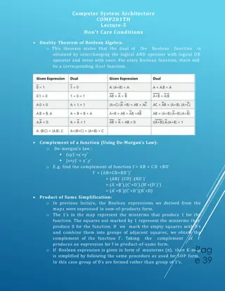
Boolean Algebra and Digital Logic


Boolean Algebra and
Digital Logic
Selecting of data or information is a critical function in
digital systems and computers
Circuits that perform selecting have:
•
A set of information inputs from which the selection is made
•
A single output
•
A set of control lines for making the selection
Logic circuits that perform selecting are called
multiplexers
Selecting can also be done by three-state logic or
transmission gates
Selecting
Multiplexers
A multiplexer selects information from an
input line and directs the information to an
output line
A typical multiplexer has
n
control inputs
(S
n
1
, … S
0
) called
selection inputs
, 2
n
information inputs (I
2
n
1
, … I
0
), and one
output Y
A multiplexer can be designed to have
m
information inputs with m
2
n
as well as
n
selection inputs
2-to-1-Line Multiplexer
Since 2 = 2
1
, n = 1
The single selection variable S has two values:
•
S = 0 selects input I
0
•
S = 1 selects input I
1
The equation:
Y = I
0
+ SI
1
The circuit:
2-to-1-Line Multiplexer
(continued)
Note the regions of the multiplexer circuit shown:
•
1-to-2-line Decoder
•
2 Enabling circuits
•
2-input OR gate
To obtain a basis for multiplexer expansion, we combine the
Enabling circuits and OR gate into a 2
2 AND-OR circuit:
•
1-to-2-line decoder
•
2
2 AND-OR
In general, for an 2
n
-to-1-line multiplexer:
•
n
-to-2
n
-line decoder
•
2
n
2 AND-OR
Example: 4-to-1-line Multiplexer
2-to-2
2
-line decoder
2
2
2 AND-OR
Multiplexer Width Expansion
Select “vectors of bits” instead of “bits”
Use multiple copies of 2
n
2 AND-OR in parallel
Example:
4-to-1-line
quad multi-
plexer
Typical Combinational Circuits – A Multiplexer (1/2)
Combinational Circuits
A
multiplexer
selects
binary information from one of many
input lines
and directs it
to a single output line
.
Selection of the particular input line, to get data from, is
controlled by a set of
selection variables
or
control lines.
Typical Combinational Circuits – A Multiplexer (2/2)
Combinational Circuits
Sequential Circuits – Introduction
Sequential Circuits
Combinational circuits are memoryless, they do not have the
concept of storage.
For some functions and operations we need to store past
values and use them in future operations – we need
sequential circuits
.
The output of a sequential circuit is a function of its inputs at
any given moment as well as its past inputs and states.
Thus sequential logic circuits must have a memory to
remember values and store previous inputs and outputs.
In order to “remember” a past state, sequential circuits rely
on feedback, where the output of a circuit is fed back as an
input to the same circuit.
Sequential Circuits - Synchronization
Timed “states”
Sequential Circuits
There are two types of sequential circuits representing two ways to
order events:
•
Asynchronous
: they become active the moment any input value
changes. C
ircuit output can change at any time (clockless)
•
Synchronous
: C
ircuit output changes only at some discrete
instants of time. Synchronization is achieved by using a timing
signal called the “
clock
” to order events.
In this course we will study synchronous sequential circuits only
Flip-Flops (1/7)
Sequential Circuits
Sequential circuits remember previous inputs by
flip-flops
.
If combinational circuits are generalizations of gates,
sequential circuits are generalizations of flip-flops.
A simple example of this concept is shown below.
•
If Q is 0 it will always be 0, if it is 1, it will always be 1.
Why?
Clock:
It
is a circuit that emits a series of pulses
•
A clock is used to decide when to update the state of the
circuit (when do “present” inputs become “past” inputs).
•
Clock speed: is generally measured in Megahertz (MHz),
or millions of pulses per second.
Synchronous Sequential Circuits: Flip-flops as state memory (2/7)
The flip-flops receive their inputs from the
combinational circuit and also from a clock signal with
pulses that occur at fixed intervals of time, as shown in
the timing diagram.
Sequential Circuits
SR Flip-Flops (3/7)
Sequential Circuits
The most basic memory unit is called an SR flip-flop.
•
The “SR” stands for set/reset.
A clocked SR flip-flop.
The output will
change only when
clock is '1', otherwise
all inputs (S and R)
will be ignored.
SR Flip-Flop Characteristics (4/7)
Sequential Circuits
How the feedback works?
•
Consider Q(t) as the value of the output Q at time t, and Q(t+1) as the
new value of Q after a new clock pulse.
•
Note also that SR flip-flop has two additional inputs S and R, in
addition to the fed-back output Q.
The behavior of an SR flip-flop is described by its
characteristic table with the two inputs S and R.
SR Flip-Flop Truth Table (5/7)
Sequential Circuits
Considering the three
inputs: S, R, and Q
,
we can
construct the truth table of
an SR flip-flop
What happens
when both S
and R are 1?
•
The output is undefined
•
We say that the SR flip-flop is
in an
unstable state
.
JK Flip-Flop (6/7)
Sequential Circuits
Jack Kilby modified the SR flip-flop to provide a
stable state
when both inputs are 1 – creating the JK flip-flop
.
The characteristic table indicates that the flip-flop is stable
for all inputs.
When both inputs are 1 the present output is
the complement (inverse) of the past output.
Try to draw the truth table of a JK flip-flop by considering the
Q feedback as well.
D Flip-Flop (7/7)
Sequential Circuits
Another modification of the SR flip-flop is the
D flip-flop
(D
stands for Data).
This sequential circuit
stores one bit of information.
When the clock is pulsed:
•
If a 1 is asserted on the input line D the output line Q becomes
a 1 (and remains 1 until the next clock pulse).
•
If a 0 is asserted on the input line the output becomes 0 (and
remains 0 until the next clock pulse).
In the realm of digital systems, selecting and directing data is essential. This involves utilizing components like multiplexers to select input lines based on control signals. Multiplexers play a key role in managing information flow within digital circuits. Combinational circuits, such as multiplexers, enable the selection of specific input lines to feed into the output line, ensuring efficient data handling within digital systems.

Uploaded on Feb 22, 2025 | 0 Views
Download Presentation

Please find below an Image/Link to download the presentation.
The content on the website is provided AS IS for your information and personal use only. It may not be sold, licensed, or shared on other websites without obtaining consent from the author.If you encounter any issues during the download, it is possible that the publisher has removed the file from their server.
You are allowed to download the files provided on this website for personal or commercial use, subject to the condition that they are used lawfully. All files are the property of their respective owners.
The content on the website is provided AS IS for your information and personal use only. It may not be sold, licensed, or shared on other websites without obtaining consent from the author.
E N D
Presentation Transcript
Boolean Algebra and Digital Logic
Selecting Selecting of data or information is a critical function in digital systems and computers Circuits that perform selecting have: A set of information inputs from which the selection is made A single output A set of control lines for making the selection Logic circuits that perform selecting are called multiplexers Selecting can also be done by three-state logic or transmission gates
Multiplexers A multiplexer selects information from an input line and directs the information to an output line A typical multiplexer has n control inputs (Sn 1, S0) called selection inputs, 2n information inputs (I2n 1, I0), and one output Y A multiplexer can be designed to have m information inputs with m 2nas well as n selection inputs
2-to-1-Line Multiplexer Since 2 = 21, n = 1 The single selection variable S has two values: S = 0 selects input I0 S = 1 selects input I1 The equation: Y = I0+ SI1 The circuit: S Enabling Circuits Decoder I0 Y S I1
2-to-1-Line Multiplexer (continued) Note the regions of the multiplexer circuit shown: 1-to-2-line Decoder 2 Enabling circuits 2-input OR gate To obtain a basis for multiplexer expansion, we combine the Enabling circuits and OR gate into a 2 2 AND-OR circuit: 1-to-2-line decoder 2 2 AND-OR In general, for an 2n-to-1-line multiplexer: n-to-2n-line decoder 2n 2 AND-OR
Example: 4-to-1-line Multiplexer 2-to-22-line decoder 22 2 AND-OR Decoder S1 43 2 AND-OR S0 Decoder Decoder S1 S1 S0 S0 I0 I1 Y Y Y I2 I3
Multiplexer Width Expansion Select vectors of bits instead of bits Use multiple copies of 2n 2 AND-OR in parallel Example: 4-to-1-line quad multi- plexer
Combinational Circuits Typical Combinational Circuits A Multiplexer (1/2) A multiplexer selects binary information from one of many input lines and directs it to a single output line. Selection of the particular input line, to get data from, is controlled by a set of selection variables or control lines.
Combinational Circuits Typical Combinational Circuits A Multiplexer (2/2)
Sequential Circuits Sequential Circuits Introduction Combinational circuits are memoryless, they do not have the concept of storage. For some functions and operations we need to store past values and use them in future operations we need sequential circuits. The output of a sequential circuit is a function of its inputs at any given moment as well as its past inputs and states. Thus sequential logic circuits must have a memory to remember values and store previous inputs and outputs. In order to remember a past state, sequential circuits rely on feedback, where the output of a circuit is fed back as an input to the same circuit.
Sequential Circuits Sequential Circuits - Synchronization Timed states There are two types of sequential circuits representing two ways to order events: Asynchronous: they become active the moment any input value changes. Circuit output can change at any time (clockless) Synchronous: Circuit output changes only at some discrete instants of time. Synchronization is achieved by using a timing signal called the clock to order events. In this course we will study synchronous sequential circuits only
Sequential Circuits Flip-Flops (1/7) Clock: Itis a circuit that emits a series of pulses A clock is used to decide when to update the state of the circuit (when do present inputs become past inputs). Clock speed: is generally measured in Megahertz (MHz), or millions of pulses per second. Sequential circuits remember previous inputs by flip-flops. If combinational circuits are generalizations of gates, sequential circuits are generalizations of flip-flops. A simple example of this concept is shown below. If Q is 0 it will always be 0, if it is 1, it will always be 1. Why?
Sequential Circuits Synchronous Sequential Circuits: Flip-flops as state memory (2/7) The flip-flops receive their inputs from the combinational circuit and also from a clock signal with pulses that occur at fixed intervals of time, as shown in the timing diagram.
Sequential Circuits SR Flip-Flops (3/7) The most basic memory unit is called an SR flip-flop. The SR stands for set/reset. A clocked SR flip-flop. The output will change only when clock is '1', otherwise all inputs (S and R) will be ignored.
Sequential Circuits SR Flip-Flop Characteristics (4/7) How the feedback works? Consider Q(t) as the value of the output Q at time t, and Q(t+1) as the new value of Q after a new clock pulse. Note also that SR flip-flop has two additional inputs S and R, in addition to the fed-back output Q. The behavior of an SR flip-flop is described by its characteristic table with the two inputs S and R.
Sequential Circuits SR Flip-Flop Truth Table (5/7) Considering the three inputs: S, R, and Q, we can construct the truth table of an SR flip-flop What happens when both S and R are 1? The output is undefined We say that the SR flip-flop is in an unstable state.
Sequential Circuits JK Flip-Flop (6/7) Jack Kilby modified the SR flip-flop to provide a stable state when both inputs are 1 creating the JK flip-flop. The characteristic table indicates that the flip-flop is stable for all inputs. When both inputs are 1 the present output is the complement (inverse) of the past output. Try to draw the truth table of a JK flip-flop by considering the Q feedback as well.
Sequential Circuits D Flip-Flop (7/7) Another modification of the SR flip-flop is the D flip-flop (D stands for Data). This sequential circuit stores one bit of information. When the clock is pulsed: If a 1 is asserted on the input line D the output line Q becomes a 1 (and remains 1 until the next clock pulse). If a 0 is asserted on the input line the output becomes 0 (and remains 0 until the next clock pulse).


")