TCAD simulation I
TCAD simulation plays a crucial role in the semiconductor industry, allowing for process and device simulations to meet market demands and reduce development time and costs. This involves modeling transport regimes, semiconductor equations, and electromagnetic fields to drive charge flow self-consis
1 views • 29 slides
Statistical Interpretation of Life Test
This presentation delves into the comparison between MIL and JEDEC requirements for semiconductor life tests, focusing on JEP001-1A, 2A, and 3A guidelines. It explores the significance of life test data, what it can demonstrate for reliability, and the importance of volume in testing. The content di
0 views • 21 slides
Exploring Growth Opportunities in Small Semiconductor Equipment Companies
Dive into the transformation of the semiconductor equipment industry from cyclical to growth-driven, backed by data from world semiconductor trade statistics, and insights from companies like Taiwan Semiconductor (TSM). Discover the increasing complexity in semiconductor packaging techniques and how
4 views • 41 slides
Semiconductor and Circuit Manufacturing Market
Semiconductor and Circuit Manufacturing Market by Component (Memory, Logic, Analog, Micro), Semiconductor (Intrinsic, Extrinsic), Material (Silicon, Germanium), Application (Consumer, Automotive, Industrial), & Geography - Global Forecast to 2031.
1 views • 5 slides

Diamond Semiconductor Substrates Market Outlook, Growth Driver
Adroit Market Research has included the Global Diamond Semiconductor Substrates Market\u00a0research to its database in order to provide a thorough analysis of the variables driving a general market growth trend.
1 views • 5 slides

15nm gold nanoparticles
The special optical, chemical, and physical characteristics of these minuscule particles are highlighted in 15nm Gold Nanoparticles Properties and Applications. Examine their important significance in emerging fields such improved materials, targeted
4 views • 10 slides

Understanding Semiconductor Sensors and their Applications
Semiconductor sensors are versatile devices that utilize semiconductor materials like silicon for detecting and measuring various non-electrical quantities. These sensors leverage the unique properties of silicon, such as high tensile strength, Young Modulus, and resistance to corrosion, making them
1 views • 26 slides
Overview of Semiconductor Materials and Applications
Understanding electronic transport in semiconductors is essential for various applications such as computers, smartphones, LEDs, and more. Semiconductors like silicon and compound semiconductors play a crucial role in creating devices with unique properties. By delving into the world of semiconducti
0 views • 20 slides

Understanding P-N Junction and Semiconductor Physics
A p-n junction is a crucial interface in semiconductor devices that consists of a p-type and an n-type material, creating a boundary with distinctive charge carriers. By doping different semiconductor materials, a p-n junction can be formed, enabling the diffusion and drift of electrons and holes ac
0 views • 25 slides
Recent Advances in Gold Nanoparticles and Nanofluids Synthesis and Applications
Gold nanoparticles (AuNPs) and nanofluids are attracting significant interest due to their unique properties and diverse applications. This article discusses the synthesis methods, optical properties, and applications of gold nanoparticles, as well as the preparation techniques and characteristics o
2 views • 8 slides
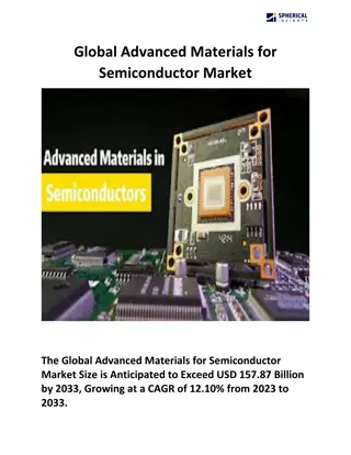
Global Advanced Materials for Semiconductor Market
\"The Global Advanced Materials for Semiconductor Market Size is Anticipated to Exceed USD 157.87 Billion by 2033, Growing at a CAGR of 12.10% from 2023 to 2033.\n\"\n
0 views • 5 slides
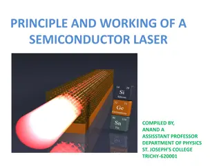
Understanding the Principle and Working of Semiconductor Lasers
Semiconductor lasers operate through absorption, spontaneous emission, and stimulated emission processes. Absorption of radiation causes electrons to jump to higher energy levels, leading to light emission. Spontaneous emission is when excited electrons return to ground state by emitting photons, wh
3 views • 17 slides
Understanding Schottky Diodes in Electronics
The Schottky diode is a semiconductor device known for its low forward voltage drop and fast switching action. Unlike ordinary diodes, it forms a metal-semiconductor junction, resulting in higher efficiency and faster switching speeds. This article explores the construction, working principle, and k
4 views • 11 slides

Understanding CMOS Layers and Interconnect Design in Semiconductor Manufacturing
This content provides detailed insights into the CMOS layers, n-well process, p-well process, twin-tub process, metal interconnect layers, gate design, and layout strategies involved in semiconductor manufacturing. Explore the images and descriptions to grasp the complexities of MOS arrays, gate con
0 views • 27 slides
Evolution of Semiconductor Devices in Modern Electronics
The lecture discusses the fundamentals of semiconductor drift and diffusion currents, diode behavior, transistor characteristics, and amplifier circuits in ECE 255. It explores the origins of modern electronics, from the invention of the bipolar transistor to the evolution of electronic devices thro
0 views • 35 slides
Chemical Vapor Deposition (CVD) Methods for Nanomaterials Characterization
Chemical Vapor Deposition (CVD) is a widely used method in the field of nanomaterial synthesis, particularly for growing nanotubes, nanowires, and nanoparticles. The process involves decomposing a gaseous precursor on a substrate with the help of a catalyst, either predeposited or provided in the ga
3 views • 8 slides

Understanding Quaternaries in Semiconductor Nanodevice Design
Learn about the treatment of quaternary materials in semiconductor nanodevice simulations, including material parameters needed for GaAs/AlGaAs heterostructures and interpolation techniques for ternaries. Explore the complexities of AlxGa1-xAsyP1-y and AlxGa1-xIn1-x-yAs quaternaries, along with the
0 views • 10 slides
Understanding Electronic Excitation in Semiconductor Nanoparticles from a Real-Space Quasiparticle Perspective
This research delves into the electronic excitation in semiconductor nanoparticles, focusing on real-space quasiparticle perspectives. It explores treating electron correlation using explicit operators, leading to faster algorithms while calculating optical gap and exciton binding energies. Various
0 views • 45 slides
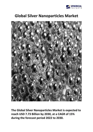
Global Silver Nanoparticles Market
The global Silver Nanoparticles Market is expected to reach USD 7.73 Billion by 2030, at a CAGR of 15% during the forecast period 2022 to 2030.
2 views • 5 slides
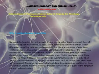
Nanotechnology and Public Health: Concerns and Developments
Nanoparticles in nanotechnology exhibit unique characteristics and behaviors that differ from microparticles, raising concerns about their impact on public health. Various applications in biomedical, cosmetic, and environmental fields highlight the potential benefits and risks associated with nanote
0 views • 6 slides
Managing E-Beam Drift for Semiconductor Fabrication
Explore techniques to address e-beam drift issues in semiconductor manufacturing, such as alignment using wafer marks and multi-pass writing strategies. Learn how to minimize drift problems and improve productivity in the fabrication process.
0 views • 44 slides
Understanding Extrinsic Semiconductors: Fermi Level and Doping Effects
Extrinsic semiconductors play a crucial role in modern electronics by allowing controlled addition of impurities to tailor conductivity. The Fermi level in extrinsic semiconductors shifts based on the number of electrons and holes in the conduction and valence bands, influencing conductivity. Doping
0 views • 14 slides
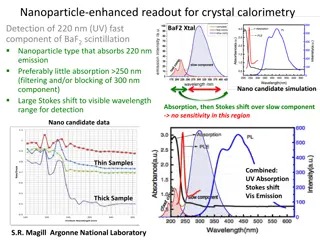
Nanoparticle-Enhanced Readout for Crystal Calorimetry: BaF2 Scintillation Detection
Nanoparticles with specific absorption and emission properties are explored to enhance the readout process for BaF2 crystal calorimetry, focusing on detecting the fast 220nm UV component. The goal is to achieve a large Stokes shift to the visible wavelength range for efficient detection, while minim
0 views • 7 slides
Understanding Semiconductor Conductivity and Scattering Mechanisms
In the study of semiconductor conductivity, the concept of degenerate and non-degenerate semiconductors is discussed, showcasing the impact of doping levels. The conductivity equation is explored in terms of electron and hole mobilities and densities. The role of scattering mechanisms, such as latti
0 views • 18 slides
Plasma Etching Challenges and Solutions in Semiconductor Fabrication
Understanding the importance of plasma etching in semiconductor fabrication, this discourse delves into the challenges faced in modeling modern etch processes. Topics covered include stochastic defect detection, reactor-level plasma physics, and an integrated model hierarchy approach. Techniques suc
0 views • 14 slides
Emerging Materials for MOS-Transistor Gate Stacks in Semiconductor Technology
Advancements in semiconductor technology necessitate the adoption of new materials for gate stacks in MOS-transistors, addressing issues like gate leakage current and gate oxide problems. With the continual scaling down of MOSFETs, the use of high-K materials offers solutions to enhance performance
0 views • 51 slides
Laser Ablation for Generation of Nanoparticles and Nanowires: Workshop Insights
Explore the latest research on laser ablation techniques for generating nanoparticles and nanowires, presented at the Si-W Ecal Workshop in Korea. Discover the various methods, applications in solar cells and LEDs, and the use of semiconductor materials. Learn about the advanced 20-TW laser system a
0 views • 31 slides
Understanding Double Patterning Lithography Techniques
Explore the world of lithography with a focus on double patterning techniques. From self-aligned double patterning to chemical vapor deposition methods, this comprehensive overview covers the key concepts, challenges, and solutions in advanced semiconductor manufacturing processes. Dive into the int
0 views • 28 slides

Role of Cell Cycle in Nanoparticle Uptake and Dilution in Cell Population
The cell cycle plays a crucial role in the cellular uptake and dilution of nanoparticles within a cell population. This process involves different phases such as G1, S, G2, and M, each with specific functions related to cell growth, DNA synthesis, protein synthesis, and cell division. Understanding
0 views • 20 slides
Nanoparticle Safety and Health Impacts: A Practical Overview
This primer discusses the safety aspects of working with nanoparticles, emphasizing the unknown properties and potential health effects. It covers routes of exposure, inhalation hazards, and examples of incidental nanoparticles impacting human health. The content stresses the importance of researche
0 views • 57 slides

Optimization Strategies for Performance-Sensitive Semiconductor Products
Discover how using JMP can optimize semiconductor product performance across various conditions, emphasizing the impact on gross margin. Learn about the benefits of Monte Carlo simulation, statistical analysis, and consistent documentation in managing complex chip designs and customer requirements e
0 views • 20 slides

Understanding Semiconductor Sensors in Sensor Technology
Introduction to semiconductor sensors, focusing on the properties of silicon that make it a preferred material for smart sensor development. Discusses the application of semiconductor sensors, planar silicon technology, and modern pressure sensors integrated with silicon diaphragms. Covers the mater
0 views • 15 slides

Semiconductor Machinery Industry Overview and Growth Analysis
Founded in 1967, a leading U.S.-based semiconductor machinery manufacturer with a 20.4% market share faces strong competition and opportunities in the evolving tech landscape. Recent news highlights industry trends, while SWOT analysis sheds light on strengths, weaknesses, opportunities, and threats
0 views • 14 slides

Understanding Fabrication Variability in Semiconductor Manufacturing
Fabrication variability in semiconductor manufacturing refers to variations in physical characteristics of transistors, impacting their electrical parameters. This variability, whether systematic or random, can lead to performance deviations in digital circuits, affecting power consumption, timing,
0 views • 48 slides
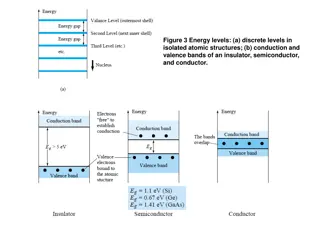
Energy Level Formation in Semiconductor Materials
Energy levels in isolated atomic structures form discrete levels which expand to bands in insulators, semiconductors, and conductors. Extrinsic materials like n-type and p-type are created by doping semiconductors with impurity atoms to alter conductivity. The n-type material involves adding pentava
0 views • 4 slides
semi conductour
The growth of the semiconductor and circuit manufacturing market is attributed to the rising acceptance of connected devices, increasing government initiatives aimed at boosting the semiconductor industry, and increasing utilization of semiconductors
1 views • 4 slides
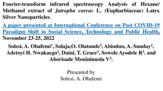
Fourier-transform Infrared Spectroscopy Analysis of Jatropha curcas Latex Silver Nanoparticles
Utilizing Fourier-transform infrared spectroscopy, this paper discusses the analysis of hexane/methanol extracts of Jatropha curcas latex silver nanoparticles. The study explores the biosynthesis of nanoparticles using plant secondary metabolites as reducing agents, highlighting the medicinal proper
0 views • 15 slides
Understanding Photolithography Process in Semiconductor Fabrication
Photolithography is a crucial step in semiconductor fabrication involving processes like exposure, development, and mask alignment. It utilizes photoresists to transfer patterns onto wafers through UV light exposure and development techniques. Positive and negative photoresists play distinct roles i
0 views • 6 slides
Exploring Nanoscience and Nanotechnology by D. Pegu
Delve into the fascinating world of nanoscience and nanotechnology as explained by D. Pegu, an associate professor at Haflong Govt. College. Learn about the fundamentals of nanophysics, nanomaterials, and nanotechnologies. Discover the impact of nanoparticles on various properties, including melting
0 views • 19 slides