Matrix Measurements and Analysis After First Metal Workshop
The pilot run matrix measurements were conducted following the 7th Belle II VXD workshop and the 18th International Workshop on DEPFET Detectors and Applications by Rainer H. Richter and Paola Avella for the MPP/HLL team. The measurements included assessing defects, diode integrity, metal shorts, and crystal defects within the matrix. Various methods such as top-side measurements and backside biasing via Punch through structure were employed to ensure the integrity of the diodes. The team was sensitive to all issues occurring in parallel to the diodes and focused on detecting shorts and crystal defects that could lead to high leakage currents.
Download Presentation

Please find below an Image/Link to download the presentation.
The content on the website is provided AS IS for your information and personal use only. It may not be sold, licensed, or shared on other websites without obtaining consent from the author. Download presentation by click this link. If you encounter any issues during the download, it is possible that the publisher has removed the file from their server.
E N D
Presentation Transcript
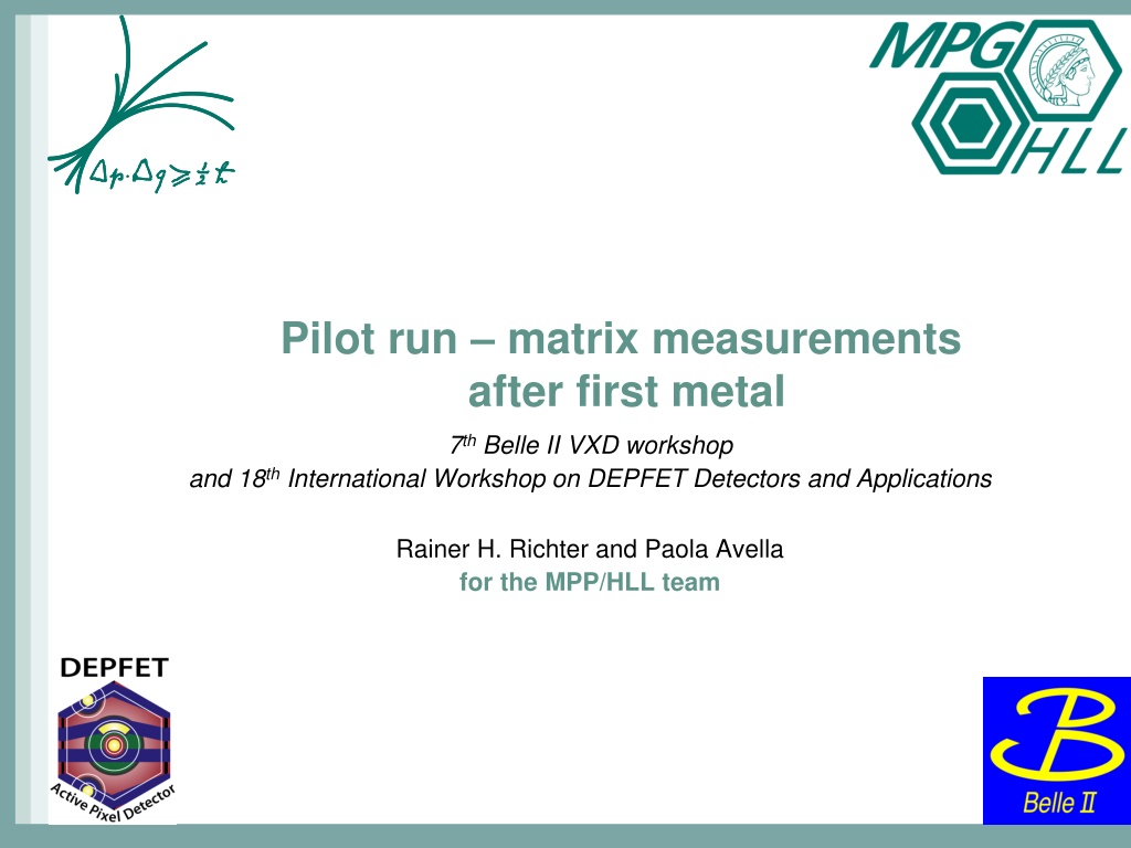
Pilot run matrix measurements after first metal 7thBelle II VXD workshop and 18thInternational Workshop on DEPFET Detectors and Applications Rainer H. Richter and Paola Avella for the MPP/HLL team
Outline IV measurements on matrices after metal 1 (limited results) - Top side measurements metal1 lines within the matrix are not yet connected (needs metal 2) Neverthess we can already check for some defects (diode integrity, some metal shorts) - Backside measurements Matrix biasing via Punch through structure makes life much easier but should work) 2 R.H. Richter, MPG HLL
Top side measurements Simple method: Connecting one p + contact and the n Bulk provides information about the integrity of all diodes within the entire matrix (experience with other project) p+ guard vs Bulk Contacts are foreseen in metal 1 3 R.H. Richter, MPG HLL
How does it works? Matrix is not depleted from the backside ! Matrix (not connected) Vguard (V-) Vguard (V-) Vbulk (0V) Vdrift= Vguard-Vpt Vdrain Early punch through at small Vbulk 75 m Backside (not directly accessible) 5cm Measurement of a lot of small diodes in parallel Drift, drains and sources are connected via punch through with small voltage differences 4 R.H. Richter, MPG HLL
We are sensitive to all what happens in parallel to the diodes N+/P+ shorts Vguard (V-) Vguard (V-) Vbulk (0V) Vdrift= Vguard-Vpt Vdrain Early punch through at small Vbulk 75 m Backside (not directly accessible) 5cm Also sensitive to crystal defects generating high leakage currents ! 5 R.H. Richter, MPG HLL
Like this: p+ drift in contact with n+ clear Lethal defect lost chip 6 R.H. Richter, MPG HLL
We are sensitive to metal 1 shorts between p+ and n+ Vguard (V-) Vguard (V-) Vbulk (0V) Vdrift= Vguard-Vpt Vdrain Early punch through at small Vbulk 75 m Backside (not directly accessible) 5cm We dont see problems between P+ regions (Drift, Drain, Source) since this does not affect the diode characteristics 7 R.H. Richter, MPG HLL
After metal 1 N+ clear line P+ source line 8 R.H. Richter, MPG HLL
Bulk vs Guard Characteristics All the long matrices of all the three project wafers show small values of current ( nA) Indication that the half ladders are in a healthy status So far 100% yield (for the testable items) 9 R.H. Richter, MPG HLL
Backside IV measurements (Punch through biassing) Vpunch through (V-) Vbulk (0V) Matrix (not connected) 75 m Backside (not directly accessible) 5cm 10 R.H. Richter, MPG HLL
Punch Through Characteristic What do we expect ? 11 R.H. Richter, MPG HLL
Punch Through Characteristic [I] Vpunch through Vbulk Phase 1 Depletion expands 1. Depletion region expanding from punchthrough contact into the bulk (small volume -> small leakage current) 12 R.H. Richter, MPG HLL
Punch Through Characteristic [II] Vpunch through Vbulk Phase 2 Backside reached bulk current Interface current 2. Depletion region reaches backside 13 R.H. Richter, MPG HLL
Punch Through Characteristic [III] Vpunch through Vbulk Phase 3: entire bulk gets depleted bulk current Interface current 3. Depletion region expands from the entire backside implant into the bulk 14 R.H. Richter, MPG HLL
Punch Through Characteristic [IV] Interface and surface currents Vpunch through Vbulk Phase 4: Active generation centers bulk current Interface current 4. generation states are getting activated generation current 15 R.H. Richter, MPG HLL
Punch Through Characteristic [V] Interface and surface currents Vpunch through Vbulk Phase 5: Generation current saturates bulk current Interface current Nice IV curve: low leakage level 5. All generation states are activated generation current saturates Operation volt. (PT) : -55V -65V 16 R.H. Richter, MPG HLL
Punch Through Characteristics all modules of wafer 35 Faster measurement: -> fluctuations Not meaningful uniform characteristics The other wafers? 17 R.H. Richter, MPG HLL
The other wafers Currents on W30 and W36 are higher Uniform wafer wise behavior: All modules of wafer 35 are fine All modules of wafer 30 and 36 are worse Not really crucial: currents are still in a moderate range But we want to know the reason 18 R.H. Richter, MPG HLL
Zoom in Current onset starts with Phase 2: depletion regions 19 R.H. Richter, MPG HLL
Punch Through Characteristics Small matrices 20 R.H. Richter, MPG HLL
Layouts of PT same design but different sizes 21 R.H. Richter, MPG HLL
Global effect concerning all modules to the entire wafer ? What is global to all modules on a wafer ?? the handle wafer We directly connected the handle wafer 22 R.H. Richter, MPG HLL
Cutting Edge (Bulk) vs Handle Wafer The current flowing between the cutting edge contact and the handle wafer for W35 is much higher than the current measured for W30 and W36. 23 R.H. Richter, MPG HLL
Punch Through Characteristics [IV] VS Cutting Edge VS Handle Wafer 24 R.H. Richter, MPG HLL
Handle wafer vs Bulk (zoom in) 25 R.H. Richter, MPG HLL
Additional measurements Not nice and rather noisy due to limited setup flexibilty in the cleanroom - Changing handle wafer potential - pos. w.r.t. bulk : no influence (up to 30V) -> no avalache - neg. w.r.t. bulk: current increase - Long term meas. high current is dropping with time 26 R.H. Richter, MPG HLL
The nature of the increased current? Handle wafer acts as backside gate - Not an avalanche current (no reaction on pos. Voltages on handle wafer) Influence of holes at the backside of the top wafer Inversion layer is connecting backside diode and cutting edge Unlikely: Handle wafer cannot become more negative than the backside p+ diode Depletion of the SIO2/Si interface (Buried oxide) The interface of the whole wafer is getting generation active - - - - - 27 R.H. Richter, MPG HLL
No significant generation current (SRH) ? in normal operation 150mm Vpunch through (V-) Vbulk (0V) good connection Electron accumulation layer - - - - - - - - - - - - - - + + + + + + + + + + + + Normal operation: handle wafer at 0V Wafer outside the module in thermal equilibrium Interface states are occupied by electrons - > very small leakage current 28 R.H. Richter, MPG HLL
Large generation current (SRH) ? If handle wafer floats 150mm Vpunch through (V-) Vbulk (0V) bad connection Electron accumulation layer disappears . . . . . . . .. . . . . . . . . . . ... . + + + + + + + + + + + + V- handle wafer floats to neg. potential by cap. coupling A few 100mV are enough Accumulation layer gets depleted Interface states are getting genaration active - > large leakage current Very good recombination lifetime in the bulk large diffusion lenghts for holes -> the whole wafer contributes Vpunch through Vbulk Phase 3: entire bulk gets depleted Small arrays are better due to their smaller backplane (Cap.) Backside pot. follows directly Vpt 29 R.H. Richter, MPG HLL
Summary and Conclusions Top side: Test for diode integrities on all modules were successful no shorts between Source and Clear lines found Backside: Badly connected handle wafer may cause parasitic gate effects leading to an increase of current We think that problem disappears if the wafers are diced (laser cut) laser melting will provide a reliable contact between handle wafer and bulk All modules of W35 (better connected) show nice IV with low leakage currents More and better measurements (setup) will follow 30 R.H. Richter, MPG HLL
