Memory Address Decoding in 8085 Microprocessor
The 8085 microprocessor with 16 address lines can access 216 locations in physical memory. Utilizing a 74LS138 address decoder, chip select signals are generated for memory block selection. The interfacing involves decoding address lines to enable memory access, with distinctions between RAM and ROM memory types. The process is illustrated through diagrams and explanations, including the use of EPROM. The article provides insights into memory structure and interface techniques.

Download Presentation

Please find below an Image/Link to download the presentation.
The content on the website is provided AS IS for your information and personal use only. It may not be sold, licensed, or shared on other websites without obtaining consent from the author. Download presentation by click this link. If you encounter any issues during the download, it is possible that the publisher has removed the file from their server.
E N D
Presentation Transcript
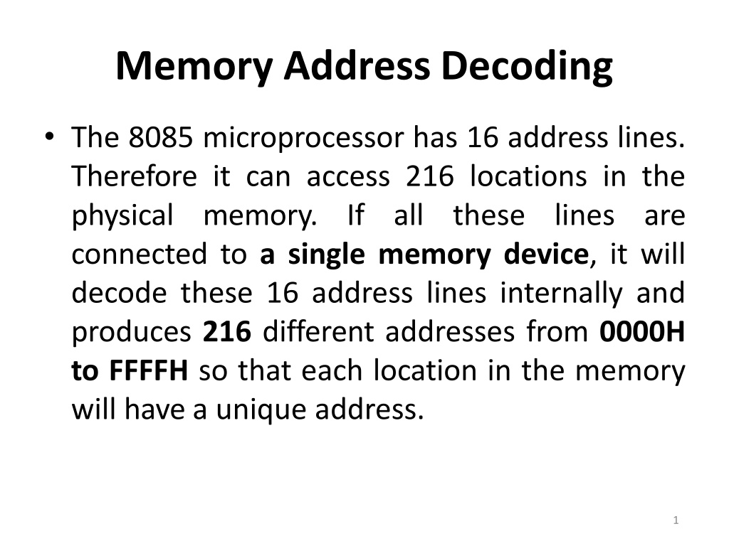
Memory Address Decoding The 8085 microprocessor has 16 address lines. Therefore it can access 216 locations in the physical memory. If all these lines are connected to a single memory device, it will decode these 16 address lines internally and produces 216 different addresses from 0000H to FFFFH so that each location in the memory will have a unique address. 1
Memory Address Decoding Fig. 1: MemoryAddress 2
74LS138 address decoder is used to generate the chip select signals for each memory block. In this decoder:- when the address lines A13, A14 and A15 are 000, the output lineY0 will be activated as shown in Fig 2. This in turn selects the first memory block. Similarly, when these lines are 001 (C=0, B=0 and A=1) Y1 will be activated and the second memory block will be selected. 3
The complete picture of the interfacing: Fig. 3: Memory Interface Diagram 5
There are two types of memory: 1. RAM: read andwrite. 2. ROM: readonly. Figure (1a) shows the R/W memory chip: 1. 2048 (2k) size. 2. 8 bit data input line and 8 bit data output line. 3. 11 address lines, A0-A10, 4. one chip select, CS. 5. RD: enable output buffer. 6. WR: enable input buffer. 7. The internal decoder is used to decode the internal memory address. 10
Figure 1b shows the typical diagram of EPROM (Erasable ProgrammableROM): 1. 2. 4096 (4k) size. A quartzwindowon it, thatuse to receive direct light to erase the program. 8 bit data output line. 12 address lines, A0-A11, One chip select,CS. RD: enable outputbuffer. The internal decoder is used to decode the internal memory address. 3. 4. 5. 6. 7. The technique to interface R/W and EPROM is the same except the EPROM does not require WR control signals. 11
Interfacing Assignment:- 1. if in the interfacing 8155 memory schematic from SDK-85 system figure (Slide 17), the address lines A10 and A9 are assumed to be 0 , A8is 1 and the O/Pline is O5. find the new memory address rang. 1. List the steps that are summarized to interface a memory with the 8085 microprocessor. (illustrate the general interfacing concept) 2. Interface 2Kbytes of Memory to 8085 with starting address 8000H. How memory interfacing can be achieved? 18