Computer Architecture: Understanding SRAM and DRAM Memory Technologies

In the field of computer architecture, SRAM and DRAM are two prevalent memory technologies with distinct characteristics. SRAM retains data as long as power is present, while DRAM is dynamic and requires data refreshing. SRAM is built with high-speed CMOS technology, whereas DRAM is more dense and built with a special process optimized for density. This article delves into the hardware structures, organization, and working principles of both SRAM and DRAM, shedding light on their differences and usage scenarios.

Download Presentation

Please find below an Image/Link to download the presentation.
The content on the website is provided AS IS for your information and personal use only. It may not be sold, licensed, or shared on other websites without obtaining consent from the author. Download presentation by click this link. If you encounter any issues during the download, it is possible that the publisher has removed the file from their server.
E N D
Presentation Transcript
CSE502: Computer Architecture CSE 502: Computer Architecture Memory / DRAM
CSE502: Computer Architecture SRAM vs. DRAM SRAM = Static RAM As long as power is present, data is retained DRAM = Dynamic RAM If you don t do anything, you lose the data SRAM: 6T per bit built with normal high-speed CMOS technology DRAM: 1T per bit (+1 capacitor) built with special DRAM process optimized for density
CSE502: Computer Architecture Hardware Structures SRAM DRAM wordline wordline Trench Capacitor b b b
CSE502: Computer Architecture DRAM Chip Organization (1/2) decoder Row Address Sense Amps Row Buffer multiplexor Column Address DRAM is much denser than SRAM
CSE502: Computer Architecture DRAM Chip Organization (2/2) Low-Level organization is very similar to SRAM Cells are only single-ended Reads destructive: contents are erased by reading Row buffer holds read data Data in row buffer is called a DRAM row Often called page - not necessarily same as OS page Read gets entire row into the buffer Block reads always performed out of the row buffer Reading a whole row, but accessing one block Similar to reading a cache line, but accessing one word
CSE502: Computer Architecture Destructive Read 1 0 sense amp output Vdd Vdd bitline voltage Sense Amp Enabled Sense Amp Enabled Wordline Enabled Wordline Enabled Vdd Vdd capacitor voltage After read of 0 or 1, cell contents close to
CSE502: Computer Architecture DRAM Read After a read, the contents of the DRAM cell are gone But still safe in the row buffer Write bits back before doing another read Reading into buffer is slow, but reading buffer is fast Try reading multiple lines from buffer (row-buffer hit) DRAM cells Sense Amps Row Buffer Process is called opening or closing a row
CSE502: Computer Architecture DRAM Refresh (1/2) Gradually, DRAM cell loses contents Even if it s not accessed This is why it s called dynamic 1 0 Gate Leakage DRAM must be regularly read and re-written What to do if no read/write to row for long time? Vdd capacitor voltage Long Time Must periodically refresh all contents
CSE502: Computer Architecture DRAM Refresh (2/2) Burst Refresh Stop the world, refresh all memory Distributed refresh Space out refresh one row at a time Avoids blocking memory for a long time Self-refresh (low-power mode) Tell DRAM to refresh itself Turn off memory controller Takes some time to exit self-refresh
CSE502: Computer Architecture Typical DRAM Access Sequence (1/5)
CSE502: Computer Architecture Typical DRAM Access Sequence (2/5)
CSE502: Computer Architecture Typical DRAM Access Sequence (3/5)
CSE502: Computer Architecture Typical DRAM Access Sequence (4/5)
CSE502: Computer Architecture Typical DRAM Access Sequence (5/5)
CSE502: Computer Architecture DRAM Read Timing Original DRAM specified Row & Column every time
CSE502: Computer Architecture DRAM Read Timing with Fast-Page Mode FPM enables multiple reads from page without RAS
CSE502: Computer Architecture SDRAM Read Timing Double-Data Rate (DDR) DRAM transfers data on both rising and falling edge of the clock SDRAM uses clock, supports bursts
CSE502: Computer Architecture Actual DRAM Signals
CSE502: Computer Architecture DRAM Signal Timing Distance matters, even at the speed of light
CSE502: Computer Architecture Examining Memory Performance Miss penalty for an 8-word cache block 1 cycle to send address 6 cycles to access each word 1 cycle to send word back ( 1 + 6 + 1) x 8 = 64 (Expensive) Wider bus option Read all words in parallel Miss penalty for 8-word block: 1 + 6 + 1 = 8
CSE502: Computer Architecture Simple Interleaved Main Memory Divide memory into n banks interleave addresses across them Bank 0 word 0 word n word 2n Bank 1 word 1 word n+1 word 2n+1 Bank 2 word 2 word n+2 word 2n+2 Bank n word n-1 word 2n-1 word 3n-1 PA Bank Word offset Access one bank while another is busy Increases bandwidth w/o a wider bus Use parallelism in memory banks to hide latency
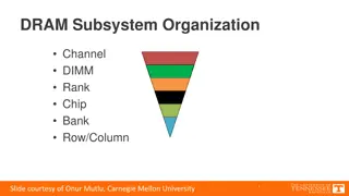
CSE502: Computer Architecture DRAM Organization All banks within the rank share all address and control pins x8 DRAM DRAM DRAM DRAM DRAM Bank All banks are independent, but can only talk to one bank at a time DRAM DRAM DRAM DRAM DIMM x8 means each DRAM outputs 8 bits, need 8 chips for DDRx (64-bit) DRAM DRAM DRAM DRAM DRAM DRAM Why 9 chips per rank? 64 bits data, 8 bits ECC x8 DRAM DRAM DRAM DRAM DRAM Rank Dual-rank x8 (2Rx8) DIMM
CSE502: Computer Architecture Memory Channels Commands Data One controller One 64-bit channel Mem Controller One controller Two 64-bit channels Mem Controller Mem Controller Two controllers Two 64-bit channels Mem Controller Use multiple channels for more bandwidth
CSE502: Computer Architecture Address Mapping Schemes (1/3) Map consecutive addresses to improve performance Multiple independent channels max parallelism Map consecutive cache lines to different channels Multiple channels/ranks/banks OK parallelism Limited by shared address and/or data pins Map close cache lines to banks within same rank Reads from same rank are faster than from different ranks Accessing rows from one bank is slowest All requests serialized, regardless of row-buffer mgmt. policies Rows mapped to same bank should avoid spatial locality Column mapping depends on row-buffer mgmt. (Why?)
CSE502: Computer Architecture Address Mapping Schemes (2/3) [ bank column ...] 0x00000 0x00100 0x00200 0x00300 0x00400 0x00500 0x00600 0x00700 0x00800 0x00900 0x00A00 0x00B00 0x00C00 0x00D00 0x00E00 0x00F00 [ column bank ] 0x00000 0x00400 0x00800 0x00C00 0x00100 0x00500 0x00900 0x00D00 0x00200 0x00600 0x00A00 0x00E00 0x00300 0x00700 0x00B00 0x00F00
CSE502: Computer Architecture Address Mapping Schemes (3/3) Example Open-page Mapping Scheme: High Parallelism: [row rank bank column channel offset] Easy Expandability: [channel rank row bank column offset] Example Close-page Mapping Scheme: High Parallelism: Easy Expandability: [row column rank bank channel offset] [channel rank row column bank offset]
CSE502: Computer Architecture CPU-to-Memory Interconnect (1/3) North Bridge can be Integrated onto CPU chip to reduce latency Figure from ArsTechnica
CSE502: Computer Architecture CPU-to-Memory Interconnect (2/3) CPU North Bridge South Bridge Discrete North and South Bridge chips
CSE502: Computer Architecture CPU-to-Memory Interconnect (3/3) South Bridge CPU Integrated North Bridge
CSE502: Computer Architecture Memory Controller (1/2) Commands Data To/From CPU Read Queue Write Queue Response Queue Scheduler Buffer Memory Controller Channel 0 Channel 1
CSE502: Computer Architecture Memory Controller (2/2) Memory controller connects CPU and DRAM Receives requests after cache misses in LLC Possibly originating from multiple cores Complicated piece of hardware, handles: DRAM Refresh Row-Buffer Management Policies Address Mapping Schemes Request Scheduling
CSE502: Computer Architecture Row-Buffer Management Policies Open-page After access, keep page in DRAM row buffer Next access to same page lower latency If access to different page, must close old one first Good if lots of locality Close-page After access, immediately close page in DRAM row buffer Next access to different page lower latency If access to different page, old one already closed Good if no locality (random access)
CSE502: Computer Architecture Request Scheduling (1/3) Write buffering Writes can wait until reads are done Queue DRAM commands Usually into per-bank queues Allows easily reordering ops. meant for same bank Common policies: First-Come-First-Served(FCFS) First-Ready First-Come-First-Served (FR-FCFS)
CSE502: Computer Architecture Request Scheduling (2/3) First-Come-First-Served Oldest request first First-Ready First-Come-First-Served Prioritize column changes over row changes Skip over older conflicting requests Find row hits (on queued reqs., even if close-page policy) Find oldest If no conflicts with in-progress request good Otherwise (if conflicts), try next oldest
CSE502: Computer Architecture Request Scheduling (3/3) Why is it hard? Tons of timing constraints in DRAM tWTR: Min. cycles before read after a write tRC: Min. cycles between consecutive open in bank Simultaneously track resources to prevent conflicts Channels, banks, ranks, data bus, address bus, row buffers Do it for many queued requests at the same time while not forgetting to do refresh
CSE502: Computer Architecture Memory-Level Parallelism (MLP) What if memory latency is 10000 cycles? Runtime dominated by waiting for memory What matters is overlapping memory accesses Memory-Level Parallelism (MLP): Average number of outstanding memory accesses when at least one memory access is outstanding. MLP is a metric Not a fundamental property of workload Dependent on the microarchitecture
CSE502: Computer Architecture AMAT with MLP If cache hit is 10 cycles (core to L1 and back) memory access is 100 cycles (core to mem and back) Then at 50% miss ratio, avg. access: 0.5 10+0.5 100 = 55 Unless MLP is >1.0, then at 50% mr,1.5 MLP,avg. access:(0.5 10+0.5 100)/1.5 = 37 at 50% mr,4.0 MLP,avg. access:(0.5 10+0.5 100)/4.0 = 14 In many cases, MLP dictates performance
CSE502: Computer Architecture Overcoming Memory Latency Caching Reduce average latency by avoiding DRAM altogether Limitations Capacity (programs keep increasing in size) Compulsory misses Memory-Level Parallelism Perform multiple concurrent accesses Prefetching Guess what will be accessed next Put in into the cache