Understanding Combinational Circuits in Computer Architecture
A combinational circuit consists of logic gates that transform binary input data into output data based on the input combination. This chapter covers the design and functionality of half-adders and full-adders, essential components in digital systems. Through truth tables, Boolean functions, and logical diagrams, the process of designing and implementing combinational circuits is explained in detail.
Download Presentation

Please find below an Image/Link to download the presentation.
The content on the website is provided AS IS for your information and personal use only. It may not be sold, licensed, or shared on other websites without obtaining consent from the author. Download presentation by click this link. If you encounter any issues during the download, it is possible that the publisher has removed the file from their server.
E N D
Presentation Transcript
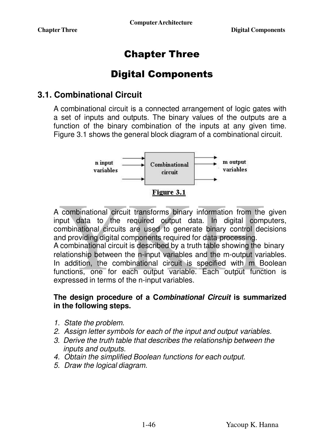
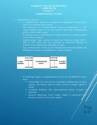
ComputerArchitecture ChapterThree Digital Components Chapter Three Digital Components 3.1. Combinational Circuit A combinational circuit is a connected arrangement of logic gates with a set of inputs and outputs. The binary values of the outputs are a function of the binary combination of the inputs at any given time. Figure 3.1 shows the general block diagram of a combinational circuit. A combinational circuit transforms binary information from the given input data to the required output data. combinational circuits are used to generate binary control decisions and providing digital components required for data processing. A combinational circuit is described by a truth table showing the binary relationship between the n-input variables and the m-output variables. In addition, the combinational circuit is specified with m Boolean functions, one for each output variable. Each output function is expressed in terms of the n-input variables. In digital computers, The design procedure of a Combinational Circuit is summarized in the following steps. 1. State the problem. 2. Assign letter symbols for each of the input and output variables. 3. Derive the truth table that describes the relationship between the inputs and outputs. 4. Obtain the simplified Boolean functions for each output. 5. Draw the logical diagram. 1-46 Yacoup K. Hanna
ComputerArchitecture ChapterThree Digital Components 1. Adders 1. Half-Adder A half-adder is a combinational circuit that performs the arithmetic addition of two bits. The input variable of the half- adder called the augend and addend bits. The output variables called Sum and Carry. The reason for specifying two output variables, since the sum of 1+1 is the binary 10, which need two bits. Recall the basic rules for binary addition as shown below. We assign symbols A and B to the two input variables Augend and Addend, S and C for the two outputs Sum and Carry. The truth table of the half-adder is as shown in table 3.1. Table 3.1 The Boolean functions for the two outputs can be obtained directly from the truth table as follows: Figure 3.2 shows the logical diagram of the half-adder and Figure 3.3 shows the logical symbol of the half-adder. 2-46 Yacoup K. Hanna
ComputerArchitecture ChapterThree Digital Components 3.1.1.2. Full-Adder A Full-Adder is a combinational circuit that forms the arithmetic sum of three input bits. It consists of three inputs and two outputs. The first two input variables, denoted by A and B, represent the two significant bits to be added, while the third input C, represent the carry from the previous lower significant position. The number of outputs must be two, since the arithmetic sum of three binary bits ranges in value from 0 to 3, and because 2 and 3 in binary is represented by two bits, therefore two outputs are needed. The two outputs are designated by the variables S for sum and CO for carry. The truth table of the Fall-adder will be as shown in table 3.2. Table 3.2 The Karnaugh maps shown in figure 3.4 are used to find logical expressions for the two outputs S and CO. 3-46 Yacoup K. Hanna
ComputerArchitecture ChapterThree Digital Components Figure 3.5 shows the logical diagram of the Fall-adder. Figure 3.6 shows the logical symbol of the Fall-adder. Homework For the full-adder of figure 3.5, determine the logic state (1 or 0) at each gate output for the following inputs: 1. A =1, B =1, and C =1 2. A = 0, B =1, andC=1 3. A = 0, B =1, andC=0 4-46 Yacoup K. Hanna
ComputerArchitecture ChapterThree Digital Components 3. Four-Bit Parallel Adders Figure 3.7 shows a Four-Bit binary parallel adder. The Four-Bit binary parallel adder works as follows: - 1. The LSB s in each binary number added go into the top- most full adder. The carry must be connected to state 0 (i.e. connected to ground) for the first full-adder. 2. The higher-adder bits are applied to the successively higher-order adders (bottom-most full adder). 3. The carry output of each adder is connected to the carry input of the next higher-order adder. 4.The output is S4 S3 S2 S1 S0 5-46 Yacoup K. Hanna
ComputerArchitecture ChapterThree Digital Components 2. Comparators The basic function of a comparator is to compare the magnitudes of two quantities and decides either as equal or different quantities. Assuming two binary numbers A and B to be compared, a comparator determines whetherA > B, B > A, or A = B. To determine the inequality of the two numbers A and B, first , the highest order bit in each number is examined through the following conditions: - 1.If A3=1 and B3= 0, then the binary number A is greater than B. 2.If A3=0 and B3= 1, then the binary number A is less than B. 3.If A3=B3, then we must examine the next lower bit position for inequality. In order to understand the logic circuitry of the comparator, consider the logical circuit of a four-bit comparator shown in figure 4.8. For our purpose, we will use two 4-bit binary numbers A and B with their general form A3A2A1A0and B3B2B1B0respectively. The A = B condition is determined by gates G1, G2, G3, G4, and G5. The outputs of the XNOR gates G1, G2, G3, and G4 are ANDed by gate G5to produce A = B. The outputs of gates G1, G2, G3, and G4 are 1 if and only if the corresponding bits of the binary numbers A and B in a specified position are the same. The A > B condition is determined by gates G6, G7, G8, G9, and G10. The outputs of gates G6, G7, G8, and G9are ORed by gate G10 to produce A > B. The outputs of gates G6, G7, G8, and G9 are 1, when the bit of the binary number A in a specified position is 1, while the corresponding bit of the binary number B is 0. The A < B condition is determined by gates G11, G12, G13, G14, and G15. The outputs of gates G11, G12, G13, and G14 are ORed by gate G15 to produce A < B. The outputs of gates G11, G12, G13, and G14are 1, when the bit of the binary number B in a specified position is 1, while the corresponding bit of the binary numberA is 0. Note. The output of G1is connected to inputs of gates G7, G8, and G9, also it is connected to the inputs of gates G12, G13, and G14. This connection provides a priority inhibit so that if the proper inequality occurs in bits A3and B3 (A3 B3), the lower-order bit checks will be inhibited. A priority inhibit is also provided by 6-46 Yacoup K. Hanna
ComputerArchitecture ChapterThree Digital Components gate G2 to gates G8, G9, G13, and G14, and by gate G3 to gates G9 and G14. Figure 3.8 Figure 3.9 shows the logic symbol for a four-bit comparator. Homework Analyze the 4-bit comparator operation shown in figure 3.8 for the two numbers A3A2A1A0 = 0111 and B3B2B1B0 =1010. 7-46 Yacoup K. Hanna
ComputerArchitecture ChapterThree Digital Components 3. Decoders A decoder is a combinational circuit that converts binary information from the n coded inputs to a maximum of 2nunique outputs. The basic function of decoder is to detect the presence of a specified combination of bits (code) on its inputs and to indicate that presence by a specified output level. Generally a decoder has n input lines to handle n bits and from one to 2noutput lines to indicate the presence of one or more n-bit combinations. 1. 2-to-4-line Decoder Figure 3.10 shows a 2-to-4-line decoder with an enable input constructed with NAND gates. The decoder is enabled when E is equal to 0 and disabled when E is equal to 1. Table 3.3 shows the 2-to-4-line decoder truth table. As indicated by the truth table, only one output is equal to 0 at any given time; the other three outputs are equal to 1. The output whose value is equal to 0 represents the equivalent binary number in inputs A1 and A0. When the circuit is disabled (i.e. E=1), no output is selected and all outputs are equal to 1. Figure 3.11 shows the logic symbol of a 2-to-4-line decoder. 8-46 Yacoup K. Hanna
ComputerArchitecture ChapterThree Digital Components Homework 1. Using NOR gates only, draw a logic diagram of a 2-to-4-line decoder. Include an enable input. 2. Modify the decoder of figure 4.10 so that the circuit is enabled when E = 1 and disabled when E = 0. List the modified truth table. 3.1.3.2. 3-to-8-line Decoder Figure 3.12 shows a 3-to-8-line decoder with an enable input E constructed with AND gates. The decoder is enabled when E is equal to 1 and disabled when E is equal to 0. Table 3.4 shows the 3-to-8-line decoder truth table. As indicated by the truth table, only one output is equal to 1 at any given time; the other seven outputs are equal to 0. The output whose value is equal to 1 represents the equivalent binary number in inputs A2, A1 and A0. When the circuit is disabled (i.e. E=0), no output is selected and all outputs are equal to 0. Notice that; in this example, the enable input is activated with 1 rather than 0 as in the example of 2-to-4- line decoder. A particular application of this decoder is a binary-to-Octal system conversion. Figure 3.12 9-46 Yacoup K. Hanna
ComputerArchitecture ChapterThree Digital Components 3.1.3.3. Decoder Expansion Sometime a certain-size decoder is needed but only smaller sizes of decoders are available, in this case we combine two or more decoders with enable inputs to form a larger decoder. For example, if a 6-to-64-line decoder is needed, it is possible to construct this decoder using four 4-to-16-line decoders. Figure 3.13 shows how a 3-to-8-line decoder is implemented using two 2-to-4-line decoders. The two least significant bits of the input are connected to both decoders. The most significant bit is connected to the enable input of one decoder and through an inverter to the enable input of the other decoder. It is assumed that each decoder is enabled when its E input is equal to 1 and disabled when E input is equal to 0. In this example when A2= 0, the upper decoder is enabled and the lower is disabled and therefore the lower decoder outputs become inactive with all outputs at 0. The outputs of the upper decoder generate outputs D0 to D3, depending on the values of A1 and A0 (while A2 = 0). When A2 = 1, the lower decoder is enabled and the upper decoder is disabled. The lower decoder output generates the binary equivalent D4to D7, depending on the values of A1and A0 (whileA2= 1). Homework Construct a 5-to-32-line decoder with four 3-to-8-line decoders with enable and one 2-to-4-line decoder. Use block diagrams only. 10-46 Yacoup K.Hanna
ComputerArchitecture ChapterThree Digital Components 3.1.3.4. BCD-to-Decimal Decoder Frequently this decoder is called a 4-line-to-10-line decoder. The BCD-to-Decimal Decoder converts each BCD code word into one of ten possible decimal digit indications. Table 3.5 shows a list of the ten BCD code words and their corresponding decoding functions. Figure 3.14 shows the logic diagram of the BCD-to-Decimal Decoder. Figure 3.15 shows the logic symbol of the BCD-to-Decimal Decoder (the 7442A integrated circuit). 11-46 Yacoup K.Hanna
ComputerArchitecture ChapterThree Digital Components 3.1.3.5. BCD-to-Seven-Segment Decoder The BCD-to-Seven-Segment Decoder has it is inputs the BCD code and provides outputs to energize Seven-Segment display devices to produce a decimal readout. Figure 3.16 shows the Seven-Segment display format in which it composed of seven elements or segments. For example to produce 2, segments a, b, g, e, and d are energized; to produce 4, segments f, g, b, and c are energized; to produce 8, all the seven segments are energized, and so on. Table 3.6 shows the activated segments for each of the ten decimal digits. Table 3.7 shows the truth table of the BCD-to-Seven- Segment Decoder. The SOP expression for each segment can be determined by using of a K. map. For example, the SOP expression for segment 12-46 Yacoup K.Hanna
ComputerArchitecture ChapterThree Digital Components a is computed as shown in figure 3.17, and implemented as shown in figure 3.18. In the same way, one can find the simplified logical expression for the remaining six segments with the logical diagram for each (Homework). Figure 3.19 shows the logical symbol of the complete seven- segment decoder. 3.1.4. Encoder An Encoder is a combinational logic circuit that essentially performs a reverse decoder function. Encoding symbols and alphabetic characters is achieved by means of encoders. 13-46 Yacoup K.Hanna
ComputerArchitecture ChapterThree Digital Components In general, encoder accepts an active level on one of its inputs representing a digit, such as a decimal or octal digit, and converts it to a coded output, such as binary or BCD. The following examples illustrate some type of encoders. Decimal to BCD Encoder This is a 10-line-to-4-line encoder, where the 10 input represents the 10 decimal digits (0, 1, 2, 3, 4, 5, 6, 7, 8, and 9) and the 4 outputs represent their corresponding BCD code as shown in figure 3.20. Table 3.8 shows the BCD code corresponding to each decimal digit. The relationship between each BCD bit and the ten decimal digits can be determined from table 3.8 as follows: - 1.A3 is 1 for decimal digits 8 or9. 2.A2 is 1 for decimal digits 4 or 5 or 6 or7. 3.A1 is 1 for decimal digits 2 or 3 or 6 or7. 4. A0 is 1 for decimal digits 1 or 3 or 5 or 7 or 9. A0 =1+3+5+7+9 A3 =8+9 A2 =4+5+6+7 A1 =2+3+6+7 14-46 Yacoup K.Hanna
ComputerArchitecture ChapterThree Digital Components The basic encoder logic expressions is a matter of ORing the appropriate decimal digit input lines to form each BCD output. Figure 3.21 shows the basic logic diagram of a decimal-to-BCD Encoder. diagram resulting from the above Note. A 0 digit input is not needed because the BCD outputs are all LOW when there are no HIGH inputs. The Decimal-to-BCD encoder is operates as follows: - 1. When HIGH level appears on one of the decimal digit input lines, the appropriate levels corresponding to that decimal digit occurs on the four BCD output lines. 2. When there are no HIGH inputs appears on any decimal digit input lines (i.e. 0-decimal digit assumed), the BCD outputs are all LOW level, which corresponds to decimal digit 0. Example. If input line 7 is HIGH (assuming all other input lines are LOW), this produce a HIGH on outputs A0, A1, and A2and LOW output on A3., which is the BCD code (0111) for decimal digit 7. 3.1.5. Code Converters Two type of code converters will be explained in this section using combinational logic circuits, these code converters are: - 15-46 Yacoup K.Hanna
