Processor Control Unit and ALU Implementation Overview

In Chapter 4, the processor's control unit and ALU are detailed in a simple implementation scheme. The ALU performs operations based on opcode values, while the control unit provides signals for various functions such as load/store, compare, and branch. Decoding techniques and control signal generation are discussed to optimize performance. The datapath with multiplexors and control lines, along with control signals, are illustrated to showcase the functioning of the control unit and ALU.

Download Presentation

Please find below an Image/Link to download the presentation.
The content on the website is provided AS IS for your information and personal use only. It may not be sold, licensed, or shared on other websites without obtaining consent from the author. Download presentation by click this link. If you encounter any issues during the download, it is possible that the publisher has removed the file from their server.
E N D
Presentation Transcript
Chapter 4 The Processor 1
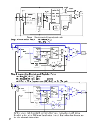
4.4 A Simple Implementation Scheme ALU Control Load/Store (LDUR/STUR): ALU computes the memory address by addition R-type instructions: ALU performs one of the four actions (AND, OR, subtract, or add), depending on the value of the 11-bit opcode field in the instruction compare and branch zero (CBZ): ALU just passes the register input value. Small control unit Input: opcode field of the instruction and a 2-bit control field, called ALUOp, with the following values: (00) indicates the operation to be performed should be add for loads and stores, (01) pass input b for CBZ, (10) determined by the operation encoded in the opcode field. Output: 4-bit signal that directly controls the ALU by generating one of the 6 combinations shown below ALU control lines 0000 0001 0010 0110 0111 1100 Function AND OR add subtract pass input b NOR 2
ALU Control ALU control inputs based on the 2-bit ALUOp control and the 11-bit opcode. ALUOp bits are generated from the main control unit. Multiple levels of decoding - common implementation technique can reduce the size of the main control unit potentially reduce the latency of the control unit ALU control 0010 0010 0111 opcode LDUR STUR CBZ ALUOp 00 00 01 Operation load register store register compare and branch on zero add subtract AND ORR Opcode field XXXXXXXXXXX XXXXXXXXXXX XXXXXXXXXXX ALU function add add pass input b R-type 10 100000 100010 100100 100101 add subtract AND OR 0010 0110 0000 0001 3
The Main Control Unit Control signals derived from instruction Opcode field: 6 11 bits wide, bit positions 31:26 to 31:21 First register operand: bit positions 9:5 (Rn) Other register operand: bit positions 20:16 (Rm), 4:0 (Rt) Another operand: 19-bit offset (CBZ) or 9-bit offset (Load/Store) The destination register for R-type instructions (Rd) and for loads (Rt) is in bit positions 4:0. 4
Datapath with control unit and control signals 7
Setting Control Signals The setting of the control lines depends only on the opcode, The table shows whether each control signal should be 0, 1, or don t care (X) for each of the opcode values 8
R-Type Instruction ADD X1,X2,X3 Four steps to execute the instruction The instruction is fetched, and the PC is incremented Two registers, X2 and X3, are read from the register file; also, the main control unit computes the setting of the control lines during this step. The ALU operates on the data read from the register file, using portions of the opcode to generate the ALU function The result from the ALU is written into the destination register (X1) in the register file. 9
Load Instruction LDUR X1, [X2, offset] Five steps to execute the instruction An instruction is fetched from the instruction memory, and the PC is incremented. A register (X2) value is read from the register file. The ALU computes the sum of the value read from the register file and the sign-extended 9 bits of the instruction (offset). The sum from the ALU is used as the address for the data memory. The data from the memory unit is written into the register file (X1). 10
CBZ Instruction CBZ X1, offset Five steps to execute the instruction An instruction is fetched from the instruction memory, and the PC is incremented. The register, X1 is read from the register file using bits 4:0 of the instruction (Rt). The ALU passes the data value read from the register file. The value of PC is added to the sign-extended, 19 bits of the instruction (offset) are shifted left by two; the result is the branch target address. The Zero status information from the ALU is used to decide which adder result to store in the PC. 11
Control Function for the simple single-cycle implementation The outputs of the control function are the control lines, and the input is the opcode field 12
Implementing Unconditional Branch 2 address Jump 31:26 25:0 Jump uses word address Update PC with concatenation of Top 4 bits of old PC 26-bit jump address 00 Need an extra control signal decoded from opcode 13
Datapath With B Added Implement a branch by storing into the PC sum of the PC and the sign extended and shifted 26-bit offset. An additional OR- gate is used with a control signal to select the branch target PC always. 14
Performance Issues Longest delay determines clock period Critical path: load instruction Instruction memory register file ALU data memory register file Not feasible to vary period for different instructions Violates design principle Making the common case fast We will improve performance by pipelining 15
4.5 An Overview of Pipelining Pipelining Analogy Pipelined laundry: overlapping execution Parallelism improves performance Pipelining improves throughput of our laundry system. When many loads of laundry to do, the improvement in throughput decreases the total time to complete the work Four loads: Speedup = 8/3.5 = 2.3 Non-stop: Speedup = 2n/0.5n + 1.5 4 = number of stages 16
LEGv8 Pipeline Five stages, one step per stage 1. IF: Instruction fetch from memory 2. ID: Instruction decode & register read 3. EX: Execute operation or calculate address 4. MEM: Access memory operand 5. WB: Write result back to register 17
Pipeline Performance Assume time for stages is 100ps for register read or write 200ps for other stages Compare pipelined datapath with single-cycle datapath The single-cycle design must allow for the slowest instruction it is LDUR so the time required for every instruction is 800 ps. Instr Instr fetch Register read ALU op Memory access 200ps Register write Total time LDUR 200ps 100 ps 200ps 100 ps 800ps STUR 200ps 100 ps 200ps 200ps 700ps R-format (ADD, SUB, AND, ORR) CBZ 200ps 100 ps 200ps 100 ps 600ps 200ps 100 ps 200ps 500ps 18
Pipeline Performance Single-cycle (Tc= 800ps) All the pipeline stages take a single clock cycle, so the clock cycle must be long enough to accommodate the slowest operation worst-case clock cycle of 200 ps Pipelined (Tc= 200ps) 19
Pipeline Speedup If all stages are balanced i.e., all take the same time Time between instructionspipelined = Time between instructionsnonpipelined Number of stages If not balanced, speedup is less Speedup due to increased throughput Latency (time for each instruction) does not decrease Pipelining improves performance by increasing instruction throughput, in contrast to decreasing the execution time of an individual instruction. Instruction throughput is the important metric because real programs execute billions of instructions. 20
Pipelining and ISA Design LEGv8 ISA designed for pipelining All instructions are 32-bits Easier to fetch and decode in one cycle c.f. x86: 1- to 15-byte instructions Few and regular instruction formats Can decode and read registers in one step Load/store addressing Can calculate address in 3rd stage, access memory in 4th stage Alignment of memory operands Memory access takes only one cycle 21