Understanding Silicon Controlled Rectifiers (SCR) in Power Electronics
Explore the world of power electronics with a focus on Silicon Controlled Rectifiers (SCR), a key component for converting and controlling power in AC or DC systems. Learn about SCR characteristics, ratings, ideal behavior, and more through detailed images and explanations.

Download Presentation

Please find below an Image/Link to download the presentation.
The content on the website is provided AS IS for your information and personal use only. It may not be sold, licensed, or shared on other websites without obtaining consent from the author. Download presentation by click this link. If you encounter any issues during the download, it is possible that the publisher has removed the file from their server.
E N D
Presentation Transcript
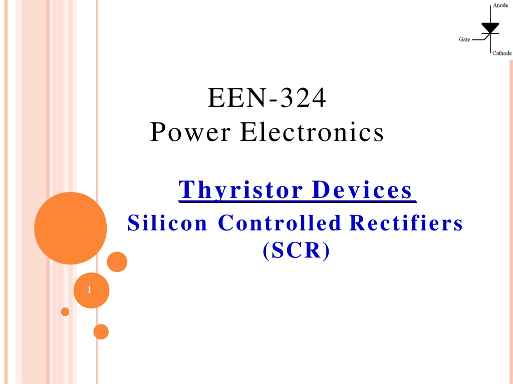
EEN-324 Power Electronics Thyristor Devices Silicon Controlled Rectifiers (SCR) 1
Power Semiconductor Switches Power Diodes Thyristors 2 layer device Device Power Transistors 3 layer Device 4 layer Thyristor devices can convert and control large amounts of power in AC or DC systems while using very low power for control. Thyristor family includes 1 Silicon controlled switch (SCR) 2Gate-turnoff thyristor (GTO) 3- Triac 4 Diac 5Silicon controlled switch (SCS) 6- Mos-controlled switch (MCT) 2
INTRODUCTION SCR is most popular of thyristor family dueto its Fast switching action , small size and high voltage and current ratings. It is commonly used in power electronicapplications. SCR has3 terminals (gate provides control) SCR is turned on by applying +ve gate sign when anode is +ve with repect to cathode. al SCR is turned off by interrupting anode current. PNPN structure Symbol 3
TWO TRANSISTOR MODEL OF SCR Gate requires small positive pulse for short duration to turn SCR on. Once the device is on, the gate signal serves no useful purpose and can be removed. 4
SCR RATINGS (a) SCR Current Ratings 1- Maximum Repetitive RMS current Rating Average on-state current is the maximum average current value that can be carried by the SCR in its on state. RMS value of nonsinusoidal waveform is simplified by approximating it by rectangular waveform. This approximation give higher RMS value, but leaves slight safety factor. 7
Average value of pulse is Form factor is 8
Knowing the form factor for given waveform, RMScurrent can be obtained from I RMS=fo(I AVE) Maximum repetitive RMS current is givenby I T(RMS)=fo(I T(AVE)) Conduction angle verses form factor Conduction angle ( ) Form factor (fo) 20 40 60 80 100 120 140 160 5.0 3.5 2.7 2.3 2.0 1.8 1.6 1.4 9
CONDUCTION ANGLE Duration for which SCR is on. It is measuredas shown 10
2- Surge Current Rating Peak anode current that SCR can handle for brief duration. 3 Latching current Minimum anode current that must flow through the SCR in order for it to stay on initially after gate signal is removed. 4 Holding Current Minimum value of anode current, required to maintain SCR in conducting state. 11
(B) SCR VOLTAGE RATINGS 1 Peak repetitive forward blockingvoltage Maximum instantaneous voltage that SCR can block in forward direction. 2 Peak Repetitive Reverse Voltage Maximum instantaneous voltage thatSCR can withstand, without breakdown, in reverse direction. 3 Non-repetitive peak reverse voltage Maximum transient reverse voltage that SCR can withstand. 12
(C) SCR RATE-OF-CHANGE RATINGS 1 (di/dt rating) Critical rate of rise of on-state current. It is the rate at which anode currentincreases and must be less than rate at which conduction area increases. To prevent damage to SCR by high di/dt value, small inductance is added in series with device. Vaue of required inductance is L>= Vp (di/dt)max 2 dv/dt rating Maximum rise time of a voltage pulse that can be applied to the SCR in the off state without causing it to fire. Unscheduled firing due to high value of dv/dt can be prevented by using RC snubber circuit. 13
(D) GATE PARAMETERS 1 Maximum Gate Peak InverseVoltage Maximum value of negative DC voltage that can be applied without damaging the gate- cathode junction. 2 Maximum Gate Trigger Current Maximum DC gate current allowed to turn on the device. 3 Maximum gate trigger voltage DC voltage necessary to produce maximum gate trigger current. 4 Maximum Gate Power Dissipation Maximum instantaneous product of gate current and gate voltage that can exist during forward-bias. 5 Minimum gate trigger voltage Minimum DC gate-to-cathode voltage required to trigger the SCR. 6-Minimum gate trigger current Minimum DC gate current necessary to turn SCR on. 14
Series and Parallel SCR Connections 15
SCRs are connected in series andparallel to extend voltage and current ratings. For high-voltage, high-current applications, series- parallel combinations of SCRs areused. 16
SCRS IN SERIES Unequal distribution of voltage across two series SCRs. Two SCRs do not share the same supply voltage. Maximum voltage that SCRs can block is V1+V2, not 2VBO. 17
Resistance equalization Voltage equalization 18
SCRS IN PARALLEL Unequal current sharing between two SCRs is shown: Total rated current of parallel connection is I1+I2, not2I2. 20
With unmatched SCRs, equal current sharing is achieved by adding low value resistor or inductor in series with each SCR, as shown below. Value of resistance R is obtainedfrom: R=V1-V2 I2-I1 21
Current sharing in SCRs with parallel reactors Equalization using resistors is inefficient dueto Extra power loss Noncompansation for unequal SCR turn-on and turn-off times. Damage due to overloading SCRs with center-tapped reactors is shownbelow. 22
SCR Gate-Triggering Circuits 23
Triggering circuits provide firing signal toturn on the SCR at precisely the correct time. Firing circuits must have following properties 1. Produce gate signal of suitable magnitude and sufficiently short rise time. 2. Produce gate signal of adequate duration. 3. Provide accurate firing control over the required range. 4. Ensure that triggering does not occur from false signals or noise 5. In AC applications, ensure that the gate signal is applied when the SCR isforward-biased 6. In three-phase circuits, provide gate pulses that are 120 apart with respect to the reference point 7. Ensure simultaneous triggering of SCRs connected in series or in parallel. 24
SCR Turnoff (Commutation) Circuits 25
What is Commutation? The process of turning off an SCRis called commutation. It is achieved by 1. Reducing anode current below holdingcurrent 2. Make anode negative withrespect to cathode Types of commutation are: 1. Natural or line commutation 2. Forced commutation 26
SCR TURNOFF METHODS Diverting the anode current to an alternate path 1. Shorting theSCR from anode to cathode 2. Applying a reverse voltage (by makingthe cathode positive with respect to the anode) across the SCR 3. Forcing the anode current to zero for a brief period 4. Opening the external path from its anode supply voltage 5. Momentarily reducing supply voltage tozero 6. 38
Other members of Thyristor Family 28
OTHER TYPES OF THYRISTORS Silicon Controlled Switch (SCS) 1. Gate Turnoff Thyristor (GTO) 2. DIAC 3. TRIAC 4. MOS-Controlled Thyristor (MCT) 5. 29
1.SCS Structure Symbol Equivalent circuit for SCS 30
(2) GTO Structure Symbol GTO Ideal VI characteristiccs 31
(3) DIAC Structure Symbol VI characteristics of diac 32
(4) TRIAC Structure Symbol SCR equivalent circuit 33


 SCR VOLTAGE RATINGS")
 SCR RATE-OF-CHANGE RATINGS")
 GATE PARAMETERS")


")


 GTO")
 DIAC")
")