Understanding the Basics of Solar Cells: Types, Materials, and Working Principles
Solar cells, also known as photovoltaic devices, convert light energy into electrical energy through the photovoltaic effect. They consist of different generations with varying materials such as crystalline silicon, cadmium telluride, and gallium arsenide. Learn about the construction, working principles, advantages, and disadvantages of solar cells in this comprehensive overview.

Download Presentation

Please find below an Image/Link to download the presentation.
The content on the website is provided AS IS for your information and personal use only. It may not be sold, licensed, or shared on other websites without obtaining consent from the author. Download presentation by click this link. If you encounter any issues during the download, it is possible that the publisher has removed the file from their server.
E N D
Presentation Transcript
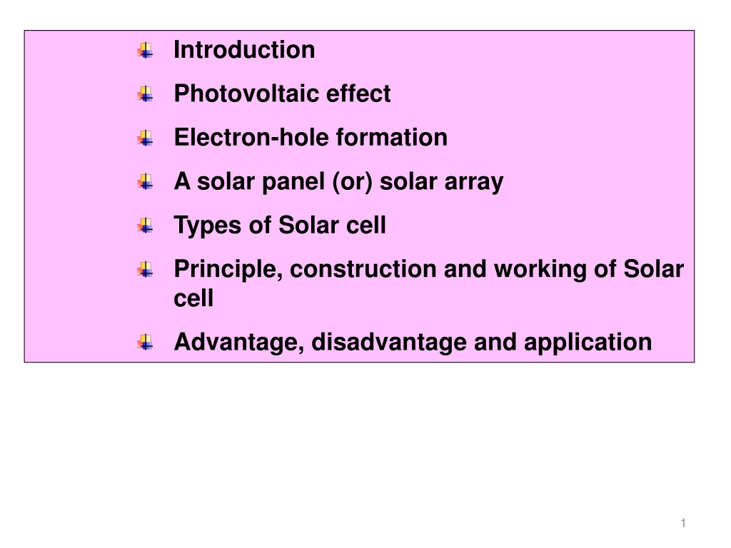
Introduction Photovoltaic effect Electron-hole formation A solar panel (or) solar array Types of Solar cell Principle, construction and working of Solar cell Advantage, disadvantage and application 1
1. Introduction Solar cell: Solar cell is a photovoltaic device that converts the light energy into electrical energy based on the principles of photovoltaic effect Recap (Lecture-1): Photo means light in Greek and Volt is the name of a pioneer in the study of electricity Alessandro Volta Albert Einstein was awarded the 1921 Nobel Prize in physics for his research on the photoelectric effect a phenomenon central to the generation of electricity through solar cells. In the early stages, the solar cell was developed only with 4 to 6 % efficiency( because of inadequate materials and problems in focusing the solar radiations). But, after 1989, the solar cells with more than 50% efficiency was developed. 2
Three generations of solar cells First Generation First generation cells consist of large-area, high quality and single junction devices. First Generation technologies involve high energy and labour inputs which prevent any significant progress in reducing production costs. 3
Second Generation Second generation materials have been developed to address energy requirements and production costs of solar cells. Alternative manufacturing techniques such as vapour deposition and electroplating are advantageous as they reduce high temperature processing significantly 4
Materials for Solar cell Solar cells are composed of various semiconducting materials 1. 2. 3. 4. 5. 6. Crystalline silicon Cadmium telluride Copper indium diselenide Gallium arsenide Indium phosphide Zinc sulphide Note: electrically conductive when supplied with light or heat, but which operate as insulators at low temperatures Semiconductors are materials, which become 5
Over 95% of all the solar cells produced worldwide are composed of the semiconductor material Silicon (Si). As the second most abundant element in earth`s crust, silicon has the advantage, of being available in sufficient quantities. To produce a solar cell, the semiconductor is contaminated or "doped". "Doping" is the intentional introduction of chemical elements into the semiconductor. By doing this, depending upon the type of dopant, one can obtain a surplus of either positive charge carriers (called p-conducting semiconductor layer) or negative charge carriers (called n-conducting semiconductor layer). 6
If two differently contaminated semiconductor layers are combined, then a so-called p-n-junction results on the boundary of the layers. p-n junction layer n-type semiconductor p- type semiconductor By doping trivalent element, we get p-type semiconductor. (with excess amount of hole) By semiconductor ( with excess amount of electron) doping pentavalent element, we get n-type 7
2. Photovoltaic effect Light energy Definition: of voltage across the PN junction semiconductor to the absorption of light radiation called photovoltaic effect. The Devices based on this effect is called photovoltaic device. The generation in a due n-type semiconductor Electrical Power is p- type semiconductor p-n junction 8
3. electron-hole formation Photovoltaic energy conversion relies on the number of photons strikes on the earth. (photon is a flux of light particles) On a clear day, about 4.4 x 10¹⁷ photons strike a square centimeter of the Earth's surface every second. Only some of these photons - those with energy in excess of the band gap - can be converted into electricity by the solar cell. When such photon enters the semiconductor, it may be absorbed and promote an electron from the valence band to the conduction band. 9
Conduction band electron Photons hole Valence band Therefore, a vacant is created in the valence band and it is called hole. Now, the electron in the conduction band and hole in valence band combine together and forms electron-hole pairs.
4. A solar panel (or) Solar array Single solar cell The sandwiched with p-type layer. single solar cell constitute the n-typpe layer The most commonly known solar cell is configured as a large-area p-n junction made from silicon wafer. A single cell can produce only very tiny amounts of electricity It can be used only to light up a small light bulb or power a calculator. Single photovoltaic cells are used in many small electronic appliances such as watches and calculators
Single Solar cell N-type P-type
Solar panel (or) solar array (or) Solar module The solar panel (or) solar array is the interconnection of number of solar module to get efficient power. A solar module consists of number of interconnected solar cells. These interconnected cells embedded between two glass plate to protect from the bad whether. Since absorption area of module is high, more energy can be produced.
5. Types of Solar cell Based on the types of crystal used, soar cells can be classified as, 1. Monocrystalline silicon cells 2. Polycrystalline silicon cells 3. Amorphous silicon cells 1. The Monocrystalline silicon cell is produced from pure silicon (single crystal). Since the Monocrystalline silicon is pure and defect free, the efficiency of cell will be higher. 2. In polycrystalline solar cell, liquid silicon is used as raw material and polycrystalline silicon was obtained followed by solidification process. The materials contain various the efficiency of this type of cell is less than Monocrystalline cell. crystalline sizes. Hence,
3. Amorphous silicon was obtained by depositing silicon film on the substrate like glass plate. The layer thickness amounts to less than 1 m the thickness of a human hair for comparison is 50-100 m. The efficiency of amorphous cells is much lower than that of the other two cell types. As a result, they are used mainly in low power equipment, such as watches and pocket calculators, or as facade elements.
Comparison of Types of solar cell Material Efficiency (%) Monocrystalline silicon 14-17 Polycrystalline silicon 13-15 Amorphous silicon 5-7
6. Principle, construction and working of Solar cell Principle: The solar cells are based on the principles of photovoltaic effect.The photovoltaic effect is the photogeneration of charge carriers in a light absorbing materials as a result of absorption of light radiation. Construction Solar cell (crystalline Silicon) consists of a n-type semiconductor (emitter) layer and p-type semiconductor layer (base). The two layers are sandwiched and hence there is formation of p-n junction. The surface is coated with anti-refection coating to avoid the loss of incident light energy due to reflection.
A proper metal contacts are made on the n-type and p- type side of the semiconductor for electrical connection Working: When a solar panel exposed to sunlight , the light energies are absorbed by a semiconduction materials. Due to this absorded enrgy, the electrons are libereted and produce the external DC current. The DC current is converted into 240-volt AC current using an inverter for different applications.
Mechanism: First, the sunlight is absorbed by a solar cell in a solar panel. The absorbed light causes electrons in the material to increase in energy. At the same time making them free to move around in the material. However, the electrons remain at this higher energy for only a short time before returning to their original lower energy position. Therefore, to collect the carriers before they lose the energy gained from the light, a PN junction is typically used.
A PN junction consists of two different regions of a semiconductor material (usually silicon), with one side called the p type region and the other the n-type region. During the incident of light energy, in p-type material, electrons can gain energy and move into the n-type region. Then they can no longer go back to their original low energy position and remain at a higher energy. The process of moving a light- generated carrier from p-type region to n-type region is called collection. These collections of carriers (electrons) can be either extracted from the device to give a current, or it can remain in the device and gives rise to a voltage.
The electrons that leave the solar cell as current give up their energy to whatever is connected to the solar cell, and then re-enter the solar cell. Once back in the solar cell, the process begins again:
The mechanism of electricity production- Different stages Conduction band High density E Valence band Low density The above diagram shows the formation of p-n junction in a solar cell. The valence band is a low-density band and conduction band is high-density band.
Stage-1 When light falls on the semiconductor surface, the electron from valence band promoted to conduction band. Therefore, (vacancy position left by the electron in the valence band) generates. Hence, there is a formation electron-hole pair on the sides junction. the hole Conduction band High density is of E of p-n Valence band Low density
Stage-2 In the stage 2, the electron and holes are diffuse across the p-n junction and there is a formation ofelectron-hole pair. Conduction band High density junction E Valence band Low density PH 0101 Unit-5 Lecture-2 27
Stage-3 In the stage 3, As electron continuous to diffuse, the negative charge build on emitter side and positive charge build on the base side. Conduction band High density junction E Valence band Low density
Stage-4 When the PN junction is connected with external circuit, the current flows. Conduction band High density junction E Power Valence band Low density
7. Advantage, disadvantage and application of Solar cell Advantage 1. It is clean and non-polluting 2. It is a renewable energy 3. Solar cells do not produce noise and they are totally silent. 4. They require very little maintenance 5. They are long lasting sources of energy which can be used almost anywhere 6. They have long life time 7. There are no fuel costs or fuel supply problems
Disadvantage 1. Solar power can not be obtained in night time 2. Solar cells (or) solar panels are very expensive 3. Energy to be stored in batteries 4. Air pollution and weather can affect the production of electricity 5. They need large area of land to produce more efficient power supply
Applications 1.Soar pumps are used for water supply. supply for appliances include 1.Domestic refrigeration, washing machine, television and lighting power 1.Ocean navigation aids: Number of lighthouses and most buoys are powered by solar cells 1.Telecommunication systems: radio transceivers on mountain tops, or telephone boxes in the country can often be solar powered 1.Electric power generation in space: To providing electrical power to satellites in an orbit around the Earth


 Solar array")

 solar array (or) Solar module")
 solar array (or) Solar module")