Understanding Transistors: Basics and Applications
Explore the world of transistors, from their construction and functioning to practical applications like switching and amplification. Learn about bipolar junction transistors and their key characteristics in this informative guide.

Download Presentation

Please find below an Image/Link to download the presentation.
The content on the website is provided AS IS for your information and personal use only. It may not be sold, licensed, or shared on other websites without obtaining consent from the author. If you encounter any issues during the download, it is possible that the publisher has removed the file from their server.
You are allowed to download the files provided on this website for personal or commercial use, subject to the condition that they are used lawfully. All files are the property of their respective owners.
The content on the website is provided AS IS for your information and personal use only. It may not be sold, licensed, or shared on other websites without obtaining consent from the author.
E N D
Presentation Transcript
HINDU COLLEGE GUNTUR
Lecture Outline Half wave Rectifier Fullwave Rectifier Bridge Rectifier
What is a transistor? A transistor is a 3 terminal electronic device made of semiconductormaterial. Transistors have many uses, including amplification, switching, voltage regulation, and the modulation of signals
Bipolar Transistor A transistor is basically a Si or Ge crystal containing three separate regions.
Architectureof BJTs The bipolar junction transistor (BJT) is constructed with three doped semiconductor regions separated by two pn junctions Regions arecalledemitter,base and collector
Bipolar Transistor The depletion layers do not have the same width, because different regions have different doping levels.
Biasing If both the junctions are forward biased free electrons enter the emitter and collector of the transistor, joins at the base and comeout of the base. If both the junction are reverse biased then small currents flows through both junctions only due to thermally produced minority carriers and surfaceleakage.
Biasing When the emitter junction is forward biased and collector junction is reverse biased then one expect large emitter current and small collector current but collector current is almost as large as emitter current.
TransistorCurrent The total current flowing into the transistor must be equal to the total current flowing out of it. ??= ??+??
TransistorApplications Switching Amplification Variable Resistor Impedance Matching Voltage Regulation
Operationof BJTs BJT will operatesin oneof followingfour region Cutoff region (for digital circuit) Saturation region (for digital circuit) Linear (active) region (to be an amplifier) Breakdown region (always be a disaster)
DC Analysis of BJTs TransistorCurrents: IE= IC+ IB alpha ( DC) IC= DCIE beta( DC) IC= DCIB DCtypicallyhas a value between20 and200
DC Analysis of BJTs DC voltages for the biased transistor: Collector voltage VC= VCC- ICRC Base voltage VB= VE+ VBE for silicontransistors,VBE= 0.7V for germanium transistors,VBE= 0.3 V
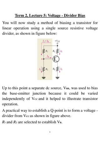
Q-point The base current, IB, is established by the base bias The point at which the base current curve intersects the dc load line is the quiescent or Q-point for the circuit
DC Analysis of BJTs The voltage divider biasing is widely used Input resistance is: RIN DCRE The base voltage is approximately: VB VCCR2/(R1+R2)