Understanding Sequential Logic Circuits and Flip-Flops
Explore the concepts of sequential logic circuits and flip-flops, including synchronous and asynchronous circuits, the basic properties of flip-flops, and the working principles of flip-flops in different input scenarios. Gain insights into the role of clock signals in synchronous circuits and the memory storage element in flip-flops.

Download Presentation

Please find below an Image/Link to download the presentation.
The content on the website is provided AS IS for your information and personal use only. It may not be sold, licensed, or shared on other websites without obtaining consent from the author. Download presentation by click this link. If you encounter any issues during the download, it is possible that the publisher has removed the file from their server.
E N D
Presentation Transcript
K.S.V.SAMBASIVARAO HEAD,DEP.OF.ELECTRONICS
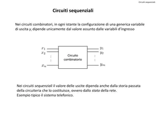
It is a combinational logic circuit with feedback i.e., previous output are present in the feedback circuit . Hence feedback circuit is known as Memory element. In sequential logic circuit present output depends on present input and also previous output Sequential logic circuits are of two types a) Synchronous b) Asynchronous a) Synchronous: The output logic circuit state was controlled by an external input signal known as clock. Hence these are known as Synchronous (or) clocked (or) timed sequential logic circuits. b) Asynchronous: The output logic state depends on previous output but not on clock pulse. Eg: Flip-flops, Registers, Counters.
Flip Flop: Generally a clocked latch is known as Flip-flop. Latch means a bistable multivibrator which stores either 0 bit (or) 1 bit. Flip flop is a single bit memory storage element and it has two outputs. The basic property of flip-flop is one output must be compliment to other ( Q!= ) Eg: R-S flip-flop, j-k flip-flop, D flip-flop, T flip-flop, Master-Slave flipflop.
It is the basic sequential circuit in flip flop. Here R means RESET and S means SET. condition. condition. WORKING: If input of first NOR Gate is R and then input of second NOR Gate is S and Q. Case 1: When R=0 and S=0 and assume previous outputs are Q=0 and =1 Input of first NOR Gate is R=0 and =1. Output of first NOR Gate is Qn+1=0=Q. Input of second NOR Gate is S=0 and Q=0. Output of second NOR Gate is Qn+1=1= . , , Output remains in its previous output state (Qn) i.e., no change If output Q=0 then flip flop is said to be in reset If output Q=1 then the flip flop is said to be in set
Case 2: When R=0 and S=1 assume previous outputs are Q=0 and ( )=1 Inputs of first NOR Gate is R=0 and =1. Output of first NOR Gate is Qn+1=0=Q. Input of second NOR Gate is S=1 and Q=0. Output of second NOR Gate is Qn+1=0= Again input of first NOR Gate is R=0 and =0 Output of first NOR Gate is Qn+1=1=Q Input of second NOR Gate is S=1 and Q=1. Output of second NOR Gate is Qn+1=0= . , , flip flop is said to be in set condition.
Case 3: When R=1 and S=0 Input of first NOR Gate is R=1 and =1. Output of first NOR Gate is Qn+1=0=Q Input of second NOR Gate is S=0 and Q=0. Output of second NOR Gate is Qn+1=1= . , , output =0 then the flip flop to be in reset condition. Case 4: When R=1,S=1 Input of first NOR Gate is R=1 and =1. Output of first NOR Gate is Qn+1=0=Q . Input of second NOR Gate is S= and Q=0. Output of second NOR Gate is Qn+1=0= . At this condition, the flip flop evaluate the basic property i.e., . Hence it is known as Forbidden (or) invalid condition.
TRUTH TABLE: R R 0 0 1 1 S S 0 1 0 1 OUTPUT(Qn+1) Qn 1 0 ? OUTPUT(Qn+1) ACTION NC SET RESET FORBIDDEN ACTION LOGIC CIRCUIT
It is a basic sequential logic circuit in flip flop R means reset and s means set. If output Q=1,the flip flop is said to be in set condition if output Q=0 then i/p is said to be in reset condition. Working:- If i/p of first NAND gate is R & ~Q and i/p of a second NAND gate is S and Q. CASE (I):When R=0 & S=0 Assume previous output are Q =0, =1 (Qn) If i/p of 2nd NAND is S=0,Q=0 o/p of NOR gates is Qn+1=Qn=1 If i/p 2nd NAND is s=0,Q=0 output of NOR is Qn+1=1= The output Qn+1 remains in the previous output state Qn that is invalid. Case(ii) :When R=0,S=1 the i/p of NAND is R=0 & Q=1 then o/p of NAND gate is Qn+1=!= Input of 2nd NAND gate is s=1& Q+0 then O/p of NAND gate is Qn+1 =1=
Case(iii): When R=1,S=0 The i/p of 1stNAND gate is R=1, =1 then output of NAND gate is Qn+1=0=~Qn The output of 2nd NAND gate is S=0,Q=0 then o/p of NAND gate is Qn+1=1=~Qn When o/p Qn+1=0 and i/p is said to be in reset condition. Case(iv): When R=1,S=1 The input of 1stNAND gate is R=1, =1 then the o/p NAND gate is Qn+1=0=Q If i/p of 2nd NAND gate is S=1,Q=0 then o/p of NAND gate is Qn+1=1= When o/p Qn+1=1 and flip-flop is said to be no change condition.
Truth table: R R S S OUTPU T(Qn+ 1) ? OUTPU T(Qn+ 1) ACTIO N N ACTIO 0 0 INVALI D RESET SET NC 0 1 1 1 0 1 0 1 Qn Logic circuit
Generally flip flops are said to be transparent. Any change in input is immediately transmitted by output logic state. In order to hold the output logic state for some duration of time we are using a external trigger pulse known as clock pulse. Hence this flip flop is known as clocked RS FLIP FLOP. By the addition of two AND gates the flip flop may be enable or disable by using external control signal known as Clock. When clock input is low output of both AND gates is low then the flip flop remains in its previous state irrespective of inputs R and S. At this condition, the flip flop is disable. When clock is high, the change in input is transmitted into the output. At his condition flip flop is enable.
Case 1:When clock is high, R=0,S=0 the output (or) remains in its previous output state. Case 2: When clock is high, R=0,S=1, then the output (or) remains in its Set condition. Case 3: When clock is high, R=1, S=0 then the output is (or) remains in its Reset condition. Case 4: When clock is high, R=1 S=1 the output is (or) it is in invalid condition.
Truth table: clock clock R R S S Output( !) !) Qn Qn 1 0 ? Output(Qn Qn+ + Action Action low High High High High X 0 0 1 1 X o 1 0 1 NC NC SET RESET Invalid Logic circuit
R-S flip flop contains two data inputs known as Reset and Set. If S=1, The flip flop is in SET condition. If R=0, Then the flip flop is said to be in RESET condition. In some applications, it is difficult to generate two data input signals to drive the outputs. Hence , the two inputs are converted as single flip flop known as D flip flop. In this flip flop, the output follows the input after some time delay when clock input is high.
WORKING: When clock is low, the flip flop remains in its previous output state i.e., Qn+1=Qn. When clock is high and D=0 , the flip flop is in RESET condition i.e., Qn+1=0. When clock is high and D=1, the flip flop is in SET condition i.e.,Qn+1=1 . Truth table cloc k k low Hig h Hig h cloc D D Output(Q n+1) Qn 0 Output(Q n+1) action action X 0 NC Reset 1 1 SET Logic circuit
It is a modified form of R-S Flip flop. It has two control inputs known as J and K. J means Set and K means Rest. The j-k flip flop eliminates the forbidden condition in R-S flip flop i.e., when clock is high J=K=1 then output i.e., Qn+1=1= n present output state is equal to compliment of previous output state. This condition is known as Toggle condition state. Positive edge triggered J-K flip flop: Case 1: When clock is low, J=K=1 then flip flop is said to be in previous output state (or) no change. Case 2: When clock is high, J=K=0 , then flip flop remains in its previous output state i.e., Qn+1=Qn. Case 3: When clock is high , J=0 K=1 , then the flip flop is in Reset condition i.e., Qn+1=0=Qn. Case 4: When clock is high , J=1 K=0 then the flip flop is in Set condition. i.e., . Qn+1=1=Qn. Case 5: When clock is high, J=K=1 then the flip flop is in toggle condition. i.e., Qn+1= n. a)In previous output , present output then flip flop is in Set condition. b) In previous output present output then the flip flop is in Rest condition
Disadvantages: When duration of clock pulse (tp) is greater than propagation delay time ( t) then output of J-K flip flop changes from 0 to 1 and 1 to 0. When J=K=1 ,(tp< t) then the output races between 0 to 1. This condition is known as Race around condition. The race around condition is eliminated when tp< t<t where tp is duration of clock pulse, t is propagation delay time of the gates, t is time period of the clock pulse. This disadvantage is eliminated by using a modified J-K flip flop known as Master Slave J-K flip flop. Truth table clo ck low Hig h Hig h Hig h Hig h clo ck J J K K output output action action X 0 X 0 Qn Qn NC NC 0 1 o Reset Logic circuit 1 0 1 SET 1 1 n Toggle


: When R=1,S=0")