Understanding Combinational Circuits through Lecture Notes
Explore the concepts of combinational logic circuits, analysis procedures, design methods, and gate-level design through lecture notes from NUS. Learn about the different classes of logic circuits, analysis procedures, and circuit design methods to enhance your understanding of digital circuits. Dive into topics like half adders, truth tables, and circuit functionality analysis.

Download Presentation

Please find below an Image/Link to download the presentation.
The content on the website is provided AS IS for your information and personal use only. It may not be sold, licensed, or shared on other websites without obtaining consent from the author. If you encounter any issues during the download, it is possible that the publisher has removed the file from their server.
You are allowed to download the files provided on this website for personal or commercial use, subject to the condition that they are used lawfully. All files are the property of their respective owners.
The content on the website is provided AS IS for your information and personal use only. It may not be sold, licensed, or shared on other websites without obtaining consent from the author.
E N D
Presentation Transcript
http://www.comp.nus.edu.sg/~cs2100/ Lecture #17 Combinational Circuits
Questions? Ask at https://sets.netlify.app/module/676ca3a07d7f5ffc1741dc65 OR Scan and ask your questions here! (May be obscured in some slides)
Aaron Tan, NUS Lecture #17: Combinational Circuits 3 Lecture #17: Combinational Circuits 1. Introduction 2. Analysis Procedure 3. Design Methods 4. Gate-Level (SSI) Design 5. Block-Level Design 6. Summary of Arithmetic Circuits 7. Example: 6-Person Voting System 8. Magnitude Comparator 9. Circuit Delays
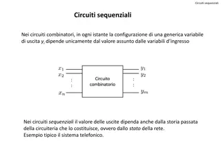
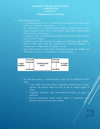
Aaron Tan, NUS Lecture #17: Combinational Circuits 4 1. Introduction Two classes of logic circuits Combinational Sequential Sequential Circuit Each output depends on both present inputs and state. Combinational Circuit Each output depends entirely on the immediate (present) inputs. Combinational Logic Combinational Logic inputs : : : : outputs inputs : : : : outputs Memory
Aaron Tan, NUS Lecture #17: Combinational Circuits 5 2. Analysis Procedure Given a combinational circuit, how do you analyze its function? What is this circuit? A+B A B F1 = (A+B).(A'+B') = (A'+B')' = A B F2 A'+B' A 0 0 1 1 B 0 1 0 1 (A+B) 0 1 1 1 (A'+B') 1 1 1 0 F1 0 1 1 0 F2 0 0 0 1 Steps: 1. Label the inputs and outputs. 2. Obtain the functions of intermediate points and the outputs. 3. Draw the truth table. 4. Deduce the functionality of the circuit Half adder.
Aaron Tan, NUS Lecture #17: Combinational Circuits 6 3. Design Methods Different combinational circuit design methods: Gate-level design method (with logic gates) Block-level design method (with functional blocks) Design methods make use of logic gates and useful function blocks These are available as Integrated Circuit (IC) chips. Types of IC chips (based on packing density): SSI, MSI, LSI, VLSI, ULSI. Main objectives of circuit design: Reduce cost (number of gates for small circuits; number of IC packages for complex circuits) Increase speed Design simplicity (re-use blocks where possible)
Aaron Tan, NUS Lecture #17: Combinational Circuits 7 4. Gate-Level (SSI) Design: Half Adder (1/2) Design procedure: 1. State problem Example: Build a Half Adder. 2. Determine and label the inputs and outputs of circuit. Example: Two inputs and two outputs labelled, as shown below. X 0 0 1 1 Y 0 1 0 1 C 0 0 0 1 S 0 1 1 0 X S Half Adder Y C (X + Y) 3. Draw the truth table.
Aaron Tan, NUS Lecture #17: Combinational Circuits 8 4. Gate-Level (SSI) Design: Half Adder (2/2) X 0 0 1 1 Y 0 1 0 1 C 0 0 0 1 S 0 1 1 0 4. Obtain simplified Boolean functions. Example: C = X Y S = X' Y + X Y' = X Y 5. Draw the logic diagram. Half Adder Block diagram of Half Adder X Y S X S Half Adder Y C C (X + Y)
Aaron Tan, NUS Lecture #17: Combinational Circuits 9 4. Gate-Level (SSI) Design: Full Adder (1/5) Half adder adds up only two bits. To add two binary numbers, we need to add 3 bits (including the carry). Example: carry X Y S 1 0 0 1 1 0 1 0 1 1 1 1 1 1 0 + Need Full Adder (so called as it can be made from two half adders). X Y Z S Full Adder C (X + Y + Z)
Aaron Tan, NUS Lecture #17: Combinational Circuits 10 4. Gate-Level (SSI) Design: Full Adder (2/5) X Y Z C S Truth table: Note: Z - carry in (to the current position) C - carry out (to the next position) 0 0 0 0 0 0 0 1 0 1 0 1 0 0 1 0 1 1 1 0 C 1 0 0 0 1 YZ 00 01 11 10 1 0 1 1 0 X 0 1 1 0 1 0 0 0 1 0 1 1 1 1 1 1 1 1 1 0 Using K-map, simplified SOP form: S YZ C = X Y + X Z + Y Z S = X' Y' Z + X' Y Z' + X Y' Z' + X Y Z 00 01 11 10 X 0 0 1 1 0 0 1 1 0 1
Aaron Tan, NUS Lecture #17: Combinational Circuits 11 4. Gate-Level (SSI) Design: Full Adder (3/5) Alternative formulae using algebraic manipulation: C = X Y + X Z + Y Z = X Y + (X + Y) Z = X Y + ( (X Y) + X Y ) Z = X Y + (X Y) Z + X Y Z = X Y + (X Y) Z S = X' Y' Z + X' Y Z' + X Y' Z' + X Y Z = X' (Y' Z + Y Z') + X (Y' Z' + Y Z) = X' (Y Z) + X (Y Z)' = X (Y Z)
Aaron Tan, NUS Lecture #17: Combinational Circuits 12 4. Gate-Level (SSI) Design: Full Adder (4/5) Circuit for above formulae: C = X Y + (X Y) Z S = X (Y Z) = (X Y) Z (XOR is associative) (X Y) X Y S (X Y) C Z Full Adder made from two Half-Adders (+ an OR gate).
Aaron Tan, NUS Lecture #17: Combinational Circuits 13 4. Gate-Level (SSI) Design: Full Adder (5/5) Circuit for above formulae: C = X Y + (X Y) Z S = X (Y Z) = (X Y) Z (XOR is associative) Block diagrams (X Y) X Y X Y Sum X Y Sum S Half Adder Half Adder (X Y) Carry Carry C Z Full Adder made from two Half-Adders (+ an OR gate).
Aaron Tan, NUS Lecture #17: Combinational Circuits 14 4. Gate-Level (SSI) Design: Code Converters Code converter takes an input code, translates to its equivalent output code. Code converter Input code Output code Example: BCD to Excess-3 code converter. Input: BCD code Output: Excess-3 code
Aaron Tan, NUS Lecture #17: Combinational Circuits 15 4. BCD to Excess-3 Code Converter (1/3) Excess-3 code 0011 0100 0101 0110 0111 1000 1001 1010 1011 1100 Digit BCD code 0 1 2 3 4 5 6 7 8 9 0000 0001 0010 0011 0100 0101 0110 0111 1000 1001
Aaron Tan, NUS Lecture #17: Combinational Circuits 16 4. BCD to Excess-3 Code Converter (2/3) Truth table: K-maps: X BCD Excess-3 W C C CD CD A B C D W X Y Z AB AB 00 01 11 10 0 0 00 01 11 10 1 0 0 0 0 0 0 0 0 1 1 1 1 00 00 0 0 1 0 0 0 1 0 1 0 0 1 1 1 1 0 0 0 01 01 0 2 0 0 1 0 0 1 0 1 B B 11 11 X X X X X X X X 3 0 0 1 1 0 1 1 0 A A 1 1 X X 0 1 X X 10 10 4 0 1 0 0 0 1 1 1 5 0 1 0 1 1 0 0 0 D D 6 0 1 1 0 1 0 0 1 Z Y 7 0 1 1 1 1 0 1 0 C C CD CD 8 1 0 0 0 1 0 1 1 AB AB 00 01 11 10 1 0 00 01 11 10 1 0 9 1 0 0 1 1 1 0 0 0 1 1 00 00 0 10 1 0 1 0 X X X X 0 1 1 1 1 01 01 0 0 0 B B 11 1 0 1 1 X X X X 11 11 X X X X X X X X 12 1 1 0 0 X X X X A A 0 1 X X 1 X X 0 10 10 13 1 1 0 1 X X X X 14 1 1 1 0 X X X X D D 15 1 1 1 1 X X X X
Aaron Tan, NUS Lecture #17: Combinational Circuits 17 4. BCD to Excess-3 Code Converter (3/3) W X C C CD CD AB AB 00 01 11 10 00 01 11 10 1 1 1 W = A + B C + B D 00 00 1 1 1 1 01 01 B B 11 11 X X X X X X X X X = B' C + B' D + B C' D' A A 1 1 X X 1 X X 10 10 D D Y = C.D + C'.D' Y Z C C CD CD AB AB 00 01 11 10 1 00 01 11 10 1 Z = D' 1 1 00 00 1 1 1 1 01 01 B B 11 11 X X X X X X X X A A 1 X X 1 X X 10 10 D D
Aaron Tan, NUS Lecture #17: Combinational Circuits 18 5. Block-Level Design More complex circuits can also be built using block-level method. In general, block-level design method (as opposed to gate-level design) relies on algorithms or formulae of the circuit, which are obtained by decomposing the main problem to sub-problems recursively (until small enough to be directly solved by blocks of circuits). First example shows how to create a 4-bit parallel adder using block-level design. Using 4-bit parallel adders as building blocks, we can create the following: 1. BCD-to-Excess-3 Code Converter 2. 16-bit Parallel Adder
Aaron Tan, NUS Lecture #17: Combinational Circuits 19 5. 4-bit Parallel Adder (1/4) Consider a circuit to add two 4-bit numbers together and a carry-in, to produce a 5-bit result. X4X3 X2X1 Y4Y3 Y2Y1 4-bit C5 C1 Parallel Adder Black-box view of 4-bit parallel adder S4S3S2S1 5-bit result is sufficient because the largest result is: 11112 + 11112 + 12 = 111112
Aaron Tan, NUS Lecture #17: Combinational Circuits 20 5. 4-bit Parallel Adder (2/4) SSI design (gate-level design) technique should not be used here. Truth table for 9 inputs is too big: 29 = 512 rows! X4X3X2X1 0 0 0 0 0 0 0 0 0 0 0 0 Y4Y3Y2Y1 0 0 0 0 0 0 0 0 0 0 0 1 C1 0 1 0 C5 0 0 0 S4S3S2S1 0 0 0 0 0 0 0 1 0 0 0 1 1 1 0 1 0 1 1 1 0 1 0 0 1 1 1 1 1 1 1 1 1 1 1 1 1 1 1 1 Simplification becomes too complicated!
Aaron Tan, NUS Lecture #17: Combinational Circuits 21 5. 4-bit Parallel Adder (3/4) Alternative design possible. Addition formula for each pair of bits (with carry in), Ci+1Si = Xi + Yi + Ci has the same function as a full adder: Ci+1 = Xi Yi + (Xi Yi) Ci Si = Xi Yi Ci C = X = Y = X + Y = 1 1 0 0 1 0 1 0 1 1 1 1 0 11 0 1
Aaron Tan, NUS Lecture #17: Combinational Circuits 22 5. 4-bit Parallel Adder (4/4) Cascading 4 full adders via their carries, we get: Y4 X4 Y3 X3 Y2 X2 Y1 X1 C4 C3 C2 C1 FA FA FA FA C5 Input Output S4 S3 S2 S1 Note that carry is propagated by cascading the carry from one full adder to the next. Called Parallel Adder because inputs are presented simultaneously (in parallel). Also called Ripple-Carry Adder.
Aaron Tan, NUS Lecture #17: Combinational Circuits 23 5. BCD to Excess-3 Converter: Revisit (1/2) BCD Excess-3 Excess-3 code can be converted from BCD code using truth table: A B C D W X Y Z 0 0 0 0 0 0 0 1 1 1 0 0 0 1 0 1 0 0 2 0 0 1 0 0 1 0 1 Gate-level design can be used since only 4 inputs. However, alternative design is possible. Use problem-specific formula: Excess-3 code = BCD Code + 00112 3 0 0 1 1 0 1 1 0 4 0 1 0 0 0 1 1 1 5 0 1 0 1 1 0 0 0 6 0 1 1 0 1 0 0 1 7 0 1 1 1 1 0 1 0 8 1 0 0 0 1 0 1 1 9 1 0 0 1 1 1 0 0 10 1 0 1 0 X X X X 11 1 0 1 1 X X X X 12 1 1 0 0 X X X X 13 1 1 0 1 X X X X 14 1 1 1 0 X X X X 15 1 1 1 1 X X X X
Aaron Tan, NUS Lecture #17: Combinational Circuits 24 5. BCD to Excess-3 Converter: Revisit (2/2) Block-level circuit: unused Cout X4 X3 X2 X1 BCD code 4-bit Parallel S4 S3 S2 S1 Adder A BCD to Excess-3 Code Converter Excess-3 code 0 0 1 1 Y4 Y3 Y2 Y1 Cin 0 Note: In the lab, input 0 (low) is connected to GND, 1 (high) to Vcc.
Aaron Tan, NUS Lecture #17: Combinational Circuits 25 5. 16-bit Parallel Adder Larger parallel adders can be built from smaller ones. Example: A 16-bit parallel adder can be constructed from four 4-bit parallel adders: X16..X13Y16..Y13 X12..X9Y12..Y9 X8..X5 Y8..Y5 X4..X1 Y4..Y1 4 4 4 4 4 4 4 4 C13 C9 C5 C1 C17 4-bit // adder 4-bit // adder 4-bit // adder 4-bit // adder 4 4 4 4 S16..S13 S12..S9 S8..S5 S4..S1 A 16-bit parallel adder 4 = S4..S1 S4S3S2S1
Aaron Tan, NUS Lecture #17: Combinational Circuits 26 6. Summary of Arithmetic Circuits (1/4) Half adder x 0 0 1 1 y C S 0 0 1 0 0 0 1 1 X S 0 1 1 0 Input bits Output bits Y C x y' x' y x y x' y' x y S = xy' + x'y S = (C+x'y')' C C x y x' y' x y x y S = x y S = (x+y)(x'+y') C C
Aaron Tan, NUS Lecture #17: Combinational Circuits 27 6. Summary of Arithmetic Circuits (2/4) x y z C 0 0 0 0 0 1 0 1 0 0 1 1 1 0 0 1 0 1 1 1 0 1 1 1 S 0 1 1 0 1 0 0 1 Full adder 0 0 0 1 0 1 1 1 A S Output bits Input bits B Cout Cin X' y' z x' y z' x y' z' x y z yz yz 00 01 11 10 00 01 11 10 x x 0 1 1 0 1 1 1 1 1 1 1 1 S C = xy + xz + yz S = x'y'z + x'yz' + xy'z' + xyz x y x y S = (x y) z x y x y x z y z C = x y + (x y) z C z
Aaron Tan, NUS Lecture #17: Combinational Circuits 28 6. Summary of Arithmetic Circuits (3/4) 4-bit parallel adder 2 ways: Subscript i Input carry Augend Addend Sum Output carry 4 0 1 0 1 0 3 1 0 0 1 0 2 1 1 1 1 1 1 0 1 1 0 1 Ci+1 Ci Ai Bi Si Serial (one FA) Parallel (n FAs for n bits) Y4 X4 Y3 X3 Y2 X2 C3 Y1 X1 C2 C4 C5 C1 FA FA FA FA Binary no. A X 4-bit sum S4 S3 S2 S1 S Binary no. B Y Cout Output carry Input carry Cin
Aaron Tan, NUS Lecture #17: Combinational Circuits 29 6. Summary of Arithmetic Circuits (4/4) Cascading 4 full adders (FAs) gives a 4-bit parallel adder. Classical method: 9 input variables 29 = 512 rows in truth table! Cascading method can be extended to larger adders. Example: 16-bit parallel adder. X16..X13Y16..Y13 X12..X9Y12..Y9 X8..X5 Y8..Y5 X4..X1 Y4..Y1 4 4 4 4 4 4 4 4 C13 C9 C5 C1 C17 4-bit // adder 4-bit // adder 4-bit // adder 4-bit // adder 4 4 4 4 S16..S13 S12..S9 S8..S5 S4..S1
Aaron Tan, NUS Lecture #17: Combinational Circuits 30 7. Example: 6-Person Voting System Application: 6-person voting system. Use FAs and a 4-bit parallel adder. Each FA can sum up to 3 votes. 0 1 0 1 1 1 0 0 A S Voter 1 Voter 2 Voter 3 1 2 3 4 1 1 0 1 0 1 A 1 1 B 1 2 3 4 3-bit Output Cout S Cin 1 2 3 4 Full-adder 1 B Cout Cin 1 0 1 0 1 1 1 1 A S Voter 4 Voter 5 Voter 6 Parallel adder 1 0 B Cout Cin Full-adder 2
Aaron Tan, NUS Lecture #17: Combinational Circuits 31 8. Magnitude Comparator (1/4) Magnitude comparator: compares 2 unsigned values A and B, to check if A>B, A=B, or A<B. To design an n-bit magnitude comparator using classical method, it would require 22n rows in truth table! We shall exploit regularity in our design. Question: How do we compare two 4-bit unsigned values A (a3a2a1a0) and B (b3b2b1b0)? If (a3 > b3) then A > B If (a3 < b3) then A < B If (a3 = b3) then if (a2 > b2)
Aaron Tan, NUS Lecture #17: Combinational Circuits 32 8. Magnitude Comparator (2/4) Let A = A3A2A1A0 , B = B3B2B1B0; xi = Ai Bi + Ai' Bi' A3 x3 A3' B3 A3 B3' B3 A3' B3 + x3 A2' B2 + x3 x2.A1' B1 + x3 x2 x1 A0' B0 A2 x2 B2 (A < B) A1 x1 A3 B3' + x3 A2 B2' + x3 x2 A1 B1' + x3 x2 x1 A0 B0' B1 A0 x0 (A > B) B0 (A = B) x3 x2 x1 x0
Aaron Tan, NUS Lecture #17: Combinational Circuits 33 8. Magnitude Comparator (3/4) Block diagram of a 4-bit magnitude comparator 4-bit Comp 4-bit Comp 0 1 1 0 A3 A2 A1 A0 0 1 1 0 A3 A2 A1 A0 1 0 1 0 B3 B2 B1 B0 (A < B) (A > B) (A = B) 1 0 0 0 0 1 1 B3 B2 B1 B0 (A < B) (A > B) (A = B) 0 1 0
Aaron Tan, NUS Lecture #17: Combinational Circuits 34 8. Magnitude Comparator (4/4) A function F accepts a 4-bit binary value ABCD, and returns 1 if 3 ABCD 12, or 0 otherwise. How would you implement F using magnitude comparators and a suitable logic gate? A B C D A3 A2 A1 A0 A0 A3 A2 A1 4-bit Comp Comp 4-bit 0 0 1 0 B3 B2 B1 B3 B2 B1 B0 B0 (A < B) (A > B) (A = B) (A = B) (A < B) (A > B) A3 A2 A1 A0 A0 A3 A2 A1 4-bit Comp Comp 4-bit F 1 1 0 1 B3 B2 B1 B0 B0 B3 B2 B1 (A < B) (A > B) (A = B) (A = B) (A < B) (A > B)
Aaron Tan, NUS Lecture #17: Combinational Circuits 35 9. Circuit Delays (1/5) Given a logic gate with delay t. If inputs are stable at times t1, t2, , tn, then the earliest time in which the output will be stable is: max( t1, t2, , tn ) + t t1 t2 : Logic Gate max (t1, t2, ..., tn ) + t : tn To calculate the delays of all outputs of a combinational circuit, repeat above rule for all gates.
Aaron Tan, NUS Lecture #17: Combinational Circuits 36 9. Circuit Delays (2/5) As a simple example, consider the full adder circuit where all inputs are available at time 0. Assume each gate has delay t. 0 max(0,0)+t = t X Y max(t,0)+t = 2t 0 S t 2t max(t,2t)+t = 3t C 0 Z Outputs S and C experience delays of 2t and 3t respectively.
Aaron Tan, NUS Lecture #17: Combinational Circuits 37 9. Circuit Delays (3/5) More complex example: 4-bit parallel adder. Y4 X4 Y3 X3 Y2 X2 Y1 X1 C4 C3 C2 0 0 0 0 0 0 0 0 0 C1 FA FA FA FA C5 S4 S3 S2 S1
Aaron Tan, NUS Lecture #17: Combinational Circuits 38 9. Circuit Delays (4/5) Analyse the delay for the repeated block. where Xi, Yi are stable at 0t, while Ci is assumed to be stable at mt. 0 0 mt Xi Yi Ci Si Ci+1 Full Adder Performing the delay calculation: 0 max(0,0)+t = t Xi Yi max(t,mt)+t 0 Si max(t,mt)+t t max(t,mt)+2t Ci+1 mt Ci
Aaron Tan, NUS Lecture #17: Combinational Circuits 39 max(t,mt)+t 0 0 mt 9. Circuit Delays (5/5) Xi Yi Ci Si Ci+1 max(t,mt)+2t Full Adder Calculating: When i=1, m=0; S1 = 2t and C2 = 3t When i=2, m=3; S2 = 4t and C3 = 5t When i=3, m=5; S3 = 6t and C4 = 7t When i=4, m=7; S4 = 8t and C5 = 9t In general, an n-bit ripple-carry parallel adder will experience the following delay times: Sn = ( (n 1)2 + 2 ) t Cn+1 = ( (n 1)2 + 3 ) t Propagation delay of ripple-carry parallel adders is proportional to the number of bits it handles. Maximum delay: ( (n 1)2 + 3 ) t
Aaron Tan, NUS Lecture #17: Combinational Circuits 40 Quick Review Questions DLD pages 128 129 Questions 6-1 to 6-4.
Aaron Tan, NUS Lecture #17: Combinational Circuits 41 End of File