Timing Effects in PICOSEC-MicroMegas Detector Study
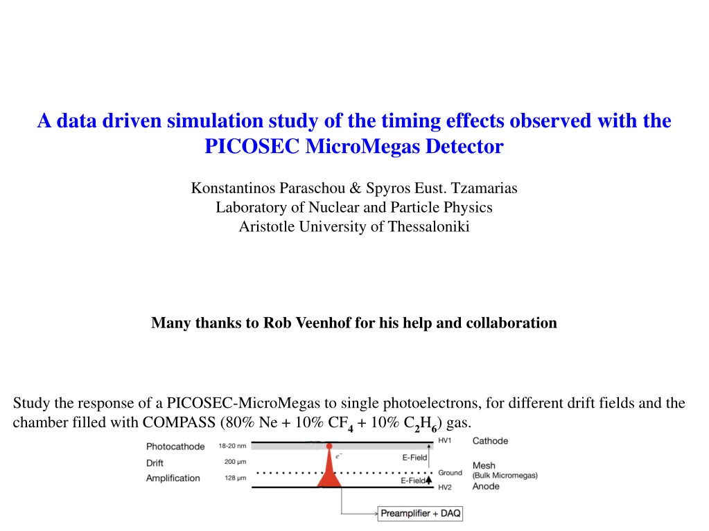

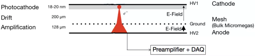
Study the response of a PICOSEC-MicroMegas to single photoelectrons, for different drift fields and the
chamber filled with COMPASS (80% Ne + 10% CF
4
+ 10% C
2
H
6
) gas.
A data driven simulation study of the timing effects observed with the
PICOSEC MicroMegas Detector
Konstantinos Paraschou & Spyros Eust. Tzamarias
Laboratory of Nuclear and Particle Physics
Aristotle University of Thessaloniki
Many thanks to Rob Veenhof for his help and collaboration
Integral
Electron-peak amplitude
Electron-peak charge
Timing (20% software CFD)
Black: Oscilloscope Data
Red: Fourier Filtered (Irrelevant)
Typical PICOSEC-
MICROMEGAS Waveform
(Experimental Data)
The e-peak amplitude and e-peak charge
distributions, corresponding to single
photoelectrons, can be parameterized
using the Polya Distribution (Red line).
The timing distributions, in narrow
bins of e-peak charge (or
amplitude) are Gaussians. However
the mean and sigma values of the
timing distributions are dependent
on the size of the e-peak
.
Mean = Signal Arrival Time (SAT)
Sigma = Time Resolution
(Experimental Data)
Fig: Signal Arrival Time dependence on
electron peak charge for different drift voltages
Fig: Time Resolution dependence on electron
peak charge for different drift voltages
Purpose of the simulation is to simulate these effects (1, 2, 3) and investigate the
mechanism that produces them.
Traditionally, the dependency of SAT on the electron peak charge is called “slewing” or “time-walk”
and is a weakness of the timing technique which is used. We use a different name because the origin of
this dependency is, in our case, physical.
Both dependencies are parameterized with a function .
b
and
w
parameters are common to
all drift voltages while
a
is common to all only for the resolution dependence.
3.) Resolution vs charge is
independent of Drift
Voltage/Field!
1.) SAT vs charge shape is
independent of Drift
Voltage/Field!
2.) Large signals
arrive earlier
that smaller ones!
(Experimental Data)
Used Garfield++ to simulate the PICOSEC
detector’s response to single photoelectrons.
Gas is COMPASS mixture
(80% Ne + 10% CF
4
+ 10% C
2
H
6
)
At 1010mbar pressure.
ANSYS model of mesh:
woven but not calendered
Drift gap = 200 μm
Amplification gap = 128 μm
Mesh Thickness = 36 μm
Amplification Voltage = 450 V → E = 35 kV/cm
Drift Voltage = 300-425 V → E in [15, 21] kV/cm
However, electronics, capacitance couplings etc.,
shape the pulse significantly. Using the
technique presented by S. Tzamarias in the
Open Lectures today, we fit the average shape of
the experimental data with the average shape of
the simulation to estimate the transfer function.
Before we search for the mechanism, we should check that the simulation gives comparable
results with the experiment, and that the effects are actually present.
Black: Experiment
Red: Fit of Simulation Transfer function to Black
S
i
m
u
l
a
t
i
o
n
E
x
p
e
r
i
m
e
n
t
S
i
g
n
a
l
A
r
r
i
v
a
l
T
i
m
e
(vs charge)
Black = Experiment
Color = Simulation
Black = Simulation
Color = Experiment
Qualitatively, we reproduce the dependence.
Signal arrival times have
been globally shifted.
S
i
m
u
l
a
t
i
o
n
E
x
p
e
r
i
m
e
n
t
After including noise, the shape of the correlations come to much better agreement.
Black = Experiment
Color = Simulation
Black = Simulation
Color = Experiment
After noise
Signal arrival times have
been globally shifted.
S
i
g
n
a
l
A
r
r
i
v
a
l
T
i
m
e
(vs charge)
+2.5 mV RMS
Uncorrelated,
Gaussian
noise
We can trim the parameters of the simulation to have an even better
agreement, but it is not our purpose at this stage.
Simulation
Experiment
Timing Resolution
(vs charge)
Black = Simulation
Color = Experiment
Black = Experiment
Color = Simulation
Before noise
Again, we reproduce the effect qualitatively.
Simulation
Experiment
Timing Resolution
Black = Experiment
Color = Simulation
Black = Simulation
Color = Experiment
After noise
+2.5 mV RMS
Uncorrelated,
Gaussian
noise
The agreement is almost perfect by simply adding some noise.
Again, we can trim the parameters of the simulation to have an even
better agreement, but it is not our purpose at this stage.
We have to scale the MC charge (or amplitude) predicted distributions in order to take into account
the electronics' gains. We expected that by adjusting the scale factor at some drift operating voltage
we should predict all the other distributions of events collected with the same anode but different
drift voltages, WITHOUT any extra fine tuning.
However…
450-400
G=27.8
450-375
G=30.2
450-425
G=21.9
It is known that the COMPASS gas mixture has a significant penning effect. Until now this effect was
ignored in the simulation. We consider different penning transfer rates to examine its behaviour.
Fig: Scale factor, G, as a function of drift voltage, divided by
the scale factor at 325 V. Red dashed lines represent linear fits.
Approximately, for a transfer rate
r ≈ 50%
,
the scale factor is not dependent on the drift
voltage setting.
Experiment
Simulation
To find the physical mechanism which produces the observed timing effects, we observed
that ultimately, the timing that is measured through the waveform analysis, is actually the
mean time at which electrons are passing through the mesh.
The mean value shift and the variation of the time distribution of all the electrons passing the
mesh are 100% correlated (slope of linear fits equal to unity) with the Signal Arrival Time
and Time Resolution dependence on the e-peak size measured by timing the e-peak pulses.
This is true for all the drift voltage settings.
Mean SAT
Mean electrons’
arrival time
vs
Number of electrons
Mean electrons’
arrival time spread
vs
Number of electrons
Whether we measure the
timing of the waveform
,
or the
mean arrival time
at which electrons pass through the mesh,
we refer to a time which exhibits the
same
characteristics.
Pre-ionization track
L
D
d
Length of the pre-amplification
avalanche.
Fig: Basic stages of the multiplication process. The initial
photoelectron, beginning at the cathode, scatters and drifts towards the
mesh/anode until a secondary electron is produced. At that point, the pre-
amplification avalanche begins its exponential development.
Cathode
Mesh
Anode
To investigate the mechanism we have to parameterize the
simulation’s results in terms of a microscopic variable.
The variable we choose is the
length of the pre-amplification
avalanche, D
.
Fig: Scatter plot of secondary electron
multiplicity vs pre-amplification
avalanche length.
Fig: Distribution of secondary
electrons’ multiplicity for pre-
amplification avalanche length in
[170μm - 175μm]
In a small region of pre-amplification avalanche
lengths, we parameterize the distribution of the
number of secondary electrons with the Polya
distribution.
We fit Polya distributions in all bins and find that both the
Mean
and the
RMS
values follow exponential laws with the
same rate parameters.
This means that the shape parameter of the Polya remains
constant across the multiplication process.
Fig:
Mean
and
RMS
values of Polya fits.
Drift Voltage = 350 V
Naturally, as the pre-amplification avalanche length increases, the time spent by the initial
photoelectron decreases while the time duration of the avalanche increases.
Although the sum of their vertical distance components of the two phenomena is constant
(always equal to the drift gap), the sum of the two times clearly depends on the length of the
avalanche.
This means that, effectively, the photoelectron and the avalanche “drift” with different velocities.
Drift Voltage = 350 V
The photoelectron before ionization and the
avalanche, move with different speeds.
The avalanche seems to move with a constant
vertical speed.
The initial photoelectron before ionization
moves much faster when the first ionization
happens early (large avalanche lengths), and
gradually “thermalizes” to the
effective speed
of the avalanche.
Fig: Effective vertical velocity as a
function of the length of the pre-
amplification avalanche.
Drift Voltage = 350 V
Naively thinking, the photoelectron must
have a large initial velocity.
Initial energy is 0.1 eV (reasonable value)
Energy acquired in the field per micron is ~2 eV/μm
Mean free path is ~7 μm.
We consider various initial conditions:
(black) isotropic direction of the emitted photoelectron from the photocathode with initial energy
of 0.1 eV,
(red) photoelectrons emmited perpendicularly to the photocathode with initial energy of 0.1 eV,
(green) 45
o
polar emission angle with initial energy of 0.1 eV,
(blue) isotropic emission direction with initial energy 0.4 eV.
Both the mean and sigma values exhibit the same dependence on the pre-amplification avalanche
length for all the above mentioned initial conditions.
This indicates that initial conditions do not play a significant role in the observed timing
dependencies.
Drift Voltage = 350 V
Figs: Effective
vertical
speed vs length of
pre-amplification avalanche. Same figs,
Left fig is zoom of right fig.
A peculiar effect is observed: the limit of the
photelectron’s speed is lower than the average
drift velocity of the avalanche for large paths.
The drift of the avalanche is a collective process in which the drift of
many electrons is averaged.
The photolectron is alone, the contribution from the transverse
movement cannot be averaged out.
Drift Voltage = 350 V
Figs: Effective
total
speed vs length of
pre-amplification avalanche. Same figs,
Left fig is zoom of right fig.
Therefore, we use the
Euclidean 3D
distance
to compute the effective
total
speed.
Indeed, the total speed thermalizes (within
statististical uncertainties) to the avalanche’s.
Drift Voltage = 350 V
450-350 V
450-400 V
450-425 V
450-350 V
450-400 V
450-425 V
Obviously, diffusion and the avalanche length (first ionization point or the Townsend a) depend on the Drift
Field, e.g. the timing spread (resolution) vs the pre-amplification avalanche length relation depends strongly
on the applied drift voltage.
The length of the pre-amplfication avalanche is not an observable variable.
To compare with experimental results, we have to re-parameterize the simulated results.
Fig: SAT vs
length of pre-amplification
avalanche
Fig: Resolution vs
length of pre-amplification
avalanche
Avalanches with the same length will not produce the same
number of electrons if the drift field is different!
450-350 V
450-400 V
450-425 V
450-350 V
450-400 V
450-425 V
The electron multiplicity in the pre-amplification avalanche is
proportional to the observed electron peak’s charge.
Therefore, we choose this variable to check that the shape of
the dependencies remain constant across different voltage
settings.
Fig: SAT vs
secondary electrons’ multiplicity of
pre-amplification avalanche
Fig: Resolution vs
secondary electrons’
multiplicity of pre-amplification avalanche
The simulation predicts that the time dependence
of the timing characteristics on the e-peak size is independent of the drift
voltage settings.
Conclusions
•
We developed a simulation tool based on Garfield++ (using Magboltz) to study the SAT
and Time Resolution dependence on the e-peak size, observed by studying the
PICOSEC-MicroMegas response to single photoelectrons.
•
The simulation describes qualitatively the observed experimental effects and,
•
we have strong indications that by trimming the parameters of the simulation (noise,
penning, etc) we can quantitatively reproduce the experimental results.
•
We have used this simulation to pinpoint the origin of the observed effects. We
concluded that the observed effects are due to the dependence of the effective drift
velocity of the primary photolectron with the distance at which it produces the first
ionization with respect to its initial position.
•
We have concluded that the reason for which the timing resolution vs e-peak size does
not seem to depend on the drift voltage, is that a larger drift field will make the time
resolution smaller but will enlarge the charge distribution, keeping the dependence
essentially the same across different drift fields.
I thank you for your attention.
Konstantinos Paraschou &
Spyros Eust. Tzamarias
Aristotle University of Thessaloniki (AUTh)
Backup Slides
Anode Voltage: 450 V
Drift Voltage: 350 V
Number of Events
This study explores the response of a PICOSEC-MicroMegas detector to single photoelectrons under various drift field conditions. The chamber is filled with COMPASS gas (80% Ne, 10% CF4, 10% C2H6). The timing effects observed in the detector are analyzed through data-driven simulations, shedding light on the detector's performance characteristics and behavior.

Download Presentation

Please find below an Image/Link to download the presentation.
The content on the website is provided AS IS for your information and personal use only. It may not be sold, licensed, or shared on other websites without obtaining consent from the author.If you encounter any issues during the download, it is possible that the publisher has removed the file from their server.
You are allowed to download the files provided on this website for personal or commercial use, subject to the condition that they are used lawfully. All files are the property of their respective owners.
The content on the website is provided AS IS for your information and personal use only. It may not be sold, licensed, or shared on other websites without obtaining consent from the author.
E N D
Presentation Transcript
A data driven simulation study of the timing effects observed with the PICOSEC MicroMegas Detector Konstantinos Paraschou & Spyros Eust. Tzamarias Laboratory of Nuclear and Particle Physics Aristotle University of Thessaloniki Many thanks to Rob Veenhof for his help and collaboration Study the response of a PICOSEC-MicroMegas to single photoelectrons, for different drift fields and the chamber filled with COMPASS (80% Ne + 10% CF4 + 10% C2H6) gas.
Typical PICOSEC- MICROMEGAS Waveform (Experimental Data) Black: Oscilloscope Data Red: Fourier Filtered (Irrelevant) Electron-peak amplitude Electron-peak charge Timing (20% software CFD) Integral
(Experimental Data) The e-peak amplitude and e-peak charge distributions, corresponding to single photoelectrons, can be parameterized using the Polya Distribution (Red line). The timing distributions, in narrow bins of e-peak amplitude) are Gaussians. However the mean and sigma values of the timing distributions are dependent on the size of the e-peak. charge (or Mean = Signal Arrival Time (SAT) Sigma = Time Resolution
(Experimental Data) 2.) Large signals arrive earlier that smaller ones! 1.) SAT vs charge shape is independent of Drift Voltage/Field! 3.) Resolution vs charge is independent of Drift Voltage/Field! Fig: Signal Arrival Time dependence on electron peak charge for different drift voltages Fig: Time Resolution dependence on electron peak charge for different drift voltages Both dependencies are parameterized with a function . b and w parameters are common to all drift voltages while a is common to all only for the resolution dependence. Traditionally, the dependency of SAT on the electron peak charge is called slewing or time-walk and is a weakness of the timing technique which is used. We use a different name because the origin of this dependency is, in our case, physical. Purpose of the simulation is to simulate these effects (1, 2, 3) and investigate the mechanism that produces them.
Used Garfield++ to simulate the PICOSEC detector s response to single photoelectrons. Gas is COMPASS mixture (80% Ne + 10% CF4 + 10% C2H6) At 1010mbar pressure. ANSYS model of mesh: woven but not calendered Drift gap = 200 m Amplification gap = 128 m Mesh Thickness = 36 m Amplification Voltage = 450 V E = 35 kV/cm Drift Voltage = 300-425 V E in [15, 21] kV/cm However, electronics, capacitance couplings etc., shape the pulse significantly. Using the technique presented by S. Tzamarias in the Open Lectures today, we fit the average shape of the experimental data with the average shape of the simulation to estimate the transfer function. Black: Experiment Red: Fit of Simulation Transfer function to Black Before we search for the mechanism, we should check that the simulation gives comparable results with the experiment, and that the effects are actually present.
Signal Arrival Time (vs charge) Simulation Experiment Black = Experiment Color = Simulation Black = Simulation Color = Experiment Qualitatively, we reproduce the dependence. Signal arrival times have been globally shifted.
Signal Arrival Time (vs charge) Simulation After noise Experiment +2.5 mV RMS Uncorrelated, Gaussian noise Black = Experiment Color = Simulation Black = Simulation Color = Experiment After including noise, the shape of the correlations come to much better agreement. We can trim the parameters of the simulation to have an even better agreement, but it is not our purpose at this stage. Signal arrival times have been globally shifted.
Timing Resolution (vs charge) Before noise Simulation Experiment Black = Simulation Color = Experiment Black = Experiment Color = Simulation Again, we reproduce the effect qualitatively.
Timing Resolution After noise Simulation Experiment +2.5 mV RMS Uncorrelated, Gaussian noise Black = Experiment Color = Simulation Black = Simulation Color = Experiment The agreement is almost perfect by simply adding some noise. Again, we can trim the parameters of the simulation to have an even better agreement, but it is not our purpose at this stage.
We have to scale the MC charge (or amplitude) predicted distributions in order to take into account the electronics' gains. We expected that by adjusting the scale factor at some drift operating voltage we should predict all the other distributions of events collected with the same anode but different drift voltages, WITHOUT any extra fine tuning. However 450-375 G=30.2 450-400 G=27.8 450-425 G=21.9 Experiment Simulation It is known that the COMPASS gas mixture has a significant penning effect. Until now this effect was ignored in the simulation. We consider different penning transfer rates to examine its behaviour. Approximately, for a transfer rate r 50%, the scale factor is not dependent on the drift voltage setting. Fig: Scale factor, G, as a function of drift voltage, divided by the scale factor at 325 V. Red dashed lines represent linear fits.
To find the physical mechanism which produces the observed timing effects, we observed that ultimately, the timing that is measured through the waveform analysis, is actually the mean time at which electrons are passing through the mesh. Mean electrons arrival time vs Number of electrons Mean SAT Mean electrons arrival time spread vs Number of electrons The mean value shift and the variation of the time distribution of all the electrons passing the mesh are 100% correlated (slope of linear fits equal to unity) with the Signal Arrival Time and Time Resolution dependence on the e-peak size measured by timing the e-peak pulses. This is true for all the drift voltage settings. Whether we measure the timing of the waveform, or the mean arrival time at which electrons pass through the mesh, we refer to a time which exhibits the same characteristics.
Cathode d L Pre-ionization track D Length of the pre-amplification avalanche. Mesh Anode Fig: Basic stages of the multiplication process. The initial photoelectron, beginning at the cathode, scatters and drifts towards the mesh/anode until a secondary electron is produced. At that point, the pre- amplification avalanche begins its exponential development. To investigate the mechanism we have to parameterize the simulation s results in terms of a microscopic variable. The variable we choose is the length of the pre-amplification avalanche, D.
Drift Voltage = 350 V Fig: Distribution of secondary electrons multiplicity for pre- amplification avalanche length in [170 m - 175 m] Fig: Scatter plot of secondary electron multiplicity vs pre-amplification avalanche length. In a small region of pre-amplification avalanche lengths, we parameterize the distribution of the number of secondary electrons with the Polya distribution. We fit Polya distributions in all bins and find that both the Mean and the RMS values follow exponential laws with the same rate parameters. This means that the shape parameter of the Polya remains constant across the multiplication process. Fig: Mean and RMS values of Polya fits.
Drift Voltage = 350 V Naturally, as the pre-amplification avalanche length increases, the time spent by the initial photoelectron decreases while the time duration of the avalanche increases. Although the sum of their vertical distance components of the two phenomena is constant (always equal to the drift gap), the sum of the two times clearly depends on the length of the avalanche. This means that, effectively, the photoelectron and the avalanche drift with different velocities.
Drift Voltage = 350 V The photoelectron before ionization and the avalanche, move with different speeds. The avalanche seems to move with a constant vertical speed. The initial photoelectron before ionization moves much faster when the first ionization happens early (large avalanche lengths), and gradually thermalizes to the effective speed of the avalanche. Fig: Effective vertical velocity as a function of the length of the pre- amplification avalanche. Naively thinking, the photoelectron must have a large initial velocity. Initial energy is 0.1 eV (reasonable value) Energy acquired in the field per micron is ~2 eV/ m Mean free path is ~7 m.
Drift Voltage = 350 V We consider various initial conditions: (black) isotropic direction of the emitted photoelectron from the photocathode with initial energy of 0.1 eV, (red) photoelectrons emmited perpendicularly to the photocathode with initial energy of 0.1 eV, (green) 45o polar emission angle with initial energy of 0.1 eV, (blue) isotropic emission direction with initial energy 0.4 eV. Both the mean and sigma values exhibit the same dependence on the pre-amplification avalanche length for all the above mentioned initial conditions. This indicates that initial conditions do not play a significant role in the observed timing dependencies.
Drift Voltage = 350 V Figs: Effective vertical speed vs length of pre-amplification avalanche. Same figs, Left fig is zoom of right fig. A peculiar effect is observed: the limit of the photelectron s speed is lower than the average drift velocity of the avalanche for large paths. The drift of the avalanche is a collective process in which the drift of many electrons is averaged. The photolectron is alone, the contribution from the transverse movement cannot be averaged out.
Drift Voltage = 350 V Figs: Effective total speed vs length of pre-amplification avalanche. Same figs, Left fig is zoom of right fig. Therefore, we use the Euclidean 3D distance to compute the effective total speed. Indeed, the total speed thermalizes (within statististical uncertainties) to the avalanche s.
450-350 V 450-400 V 450-425 V 450-350 V 450-400 V 450-425 V Fig: Resolution vs length of pre-amplification avalanche Fig: SAT vs length of pre-amplification avalanche Obviously, diffusion and the avalanche length (first ionization point or the Townsend a) depend on the Drift Field, e.g. the timing spread (resolution) vs the pre-amplification avalanche length relation depends strongly on the applied drift voltage. Avalanches with the same length will not produce the same number of electrons if the drift field is different! The length of the pre-amplfication avalanche is not an observable variable. To compare with experimental results, we have to re-parameterize the simulated results.
450-350 V 450-400 V 450-425 V 450-350 V 450-400 V 450-425 V Fig: Resolution vs secondary electrons multiplicity of pre-amplification avalanche Fig: SAT vs secondary electrons multiplicity of pre-amplification avalanche The electron multiplicity in the pre-amplification avalanche is proportional to the observed electron peak s charge. Therefore, we choose this variable to check that the shape of the dependencies remain constant across different voltage settings. The simulation predicts that the time dependence of the timing characteristics on the e-peak size is independent of the drift voltage settings.
Conclusions We developed a simulation tool based on Garfield++ (using Magboltz) to study the SAT and Time Resolution dependence on the e-peak size, observed by studying the PICOSEC-MicroMegas response to single photoelectrons. The simulation describes qualitatively the observed experimental effects and, we have strong indications that by trimming the parameters of the simulation (noise, penning, etc) we can quantitatively reproduce the experimental results. We have used this simulation to pinpoint the origin of the observed effects. We concluded that the observed effects are due to the dependence of the effective drift velocity of the primary photolectron with the distance at which it produces the first ionization with respect to its initial position. We have concluded that the reason for which the timing resolution vs e-peak size does not seem to depend on the drift voltage, is that a larger drift field will make the time resolution smaller but will enlarge the charge distribution, keeping the dependence essentially the same across different drift fields. I thank you for your attention. Konstantinos Paraschou & Spyros Eust. Tzamarias Aristotle University of Thessaloniki (AUTh)
Anode Voltage: 450 V Drift Voltage: 350 V


")
")


 predicted")