Phase-Locked Loops: Electronic Circuit Applications

College of Engineering stage / third
Dept. of the electrical power and Machine Date: THR24/3/2016
Subject/ ELECTRONIC SYSTEMS Time/ 2 hour
s
PHASE-LOCKED LOOP
By
Assist. Lecturer AMMAR ISSA ISMAEL
Lecture 4
The Reference :Electronic Devices and Circuit
Theory

PHASE-LOCKED LOOP
•
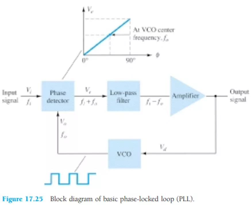
A phase-locked loop (PLL) is an electronic circuit that consists of a
phase
detector
,
a low-pass filter
, and a
voltage-controlled oscillator
connected as
shown in Fig. 17.25.
PHASE-LOCKED LOOP
Common applications of a PLL include:
•
(1) frequency synthesizers that provide multiples of a reference signal frequency
[e.g., the carrier frequency for the multiple channels of a citizens ’ band (CB) unit
or marine-radio-band unit can be generated using a single-crystal-controlled
frequency and its multiples generated using a PLL];
•
(2) FM demodulation networks for FM operation with excellent linearity between
the input signal frequency and the PLL output voltage;
•
(3) demodulation of the two data transmission or carrier frequencies in digital-data
transmission used in frequency-shift keying (FSK) operation; and
•
(4) a wide variety of areas including modems, telemetry receivers and
transmitters, tone decoders, AM detectors, and tracking filters
PHASE-LOCKED LOOP
•
An input signal, Vi, and that from a VCO, Vo, are compared by a phase
comparator (refer to Fig. 17.25) providing an output voltage, Ve, that
represents the
phase difference
between the two signals. This voltage is
then fed to a low-pass filter that provides an output voltage (amplified if
necessary) that can be taken as the output voltage from the PLL and is used
internally as the voltage to modulate the VCO ’s frequency. The closed-
loop operation of the circuit is to maintain the VCO frequency locked to
that of the input signal frequency.
Basic PLL Operation
•
The basic operation of a PLL circuit can be explained using the circuit of Fig. 17.25 as
reference.
•
We will first consider the operation of the various circuits in the phase-locked loop when
the loop is operating in
lock
(the input signal frequency and the VCO frequency are the
same). When the input signal frequency is the same as that from the VCO to the
comparator, the voltage, Vd, taken as output is the value needed to hold the VCO in lock
with the input signal. The VCO then provides output of affixed amplitude square-wave
signal at the frequency of the input. Best operation is obtained if the VCO center
frequency, fo, is set with the dc bias voltage midway in its linear operating range. The
amplifier allows this adjustment in dc voltage from that obtained as output of the filter
circuit. When the loop is in lock, the two signals to the comparator are of the same
frequency, although not
necessarily in phase.
A fixed phase difference between the two
signals to the comparator results in a fixed dc voltage to the VCO
Basic PLL Operation
•
Changes in the input signal frequency then result in change in the dc voltage
to the VCO. Within a capture-and-lock frequency range, the dc voltage will
drive the VCO frequency to match that of the input While the loop is trying to
achieve lock, the output of the phase comparator contains frequency
components at the sum and difference of the signals compared.
•
A low-pass filter passes only the lower-frequency component of the signal so
that the loop can obtain lock between input and VCO signals.
•
Owing to the limited operating range of the VCO and the feedback connection
of the PLL circuit, there are two important frequency bands specified for a
PLL. The capture range of a PLL is the frequency range centered about the
VCO free-running frequency, fo, over which the loop can acquire lock with
the input signal. Once the PLL has achieved capture, it can maintain lock with
the input signal over a somewhat wider frequency range called the lock range.
Applications
•
The PLL can be used in a wide variety of
applications, including
•
(1) frequency demodulation,
•
(2) frequency synthesis,
•
(3) FSK decoders.
FREQUENCY DEMODULATION
•
FM demodulation or detection can be directly achieved using the PLL
circuit. If the PLL center frequency is selected or designed at the FM
carrier frequency, the filtered or output voltage of the circuit of Fig. 17.25
is the desired demodulated voltage, varying in value proportional to the
variation of the signal frequency.
•
The PLL circuit thus operates as a complete intermediate-frequency (IF)
strip, limiter, and demodulator as used in FM receivers
FREQUENCY DEMODULATION
•
One popular PLL unit is the 565, shown in Fig. 17.26a. The 565 contains a
1- phase detector, 2- amplifier, 3- voltage-controlled oscillator,
•
An external resistor and capacitor, R1 and C1, are used to set the free-
running or center frequency of the VCO.
•
Another external capacitor, C2, is used to set the low-pass filter passband,
•
the VCO output must be connected back as input to the phase detector to
close the PLL loop.
•
The 565 typically uses two power supplies, V
+
and V
-
Figure 17.26b shows the PLL connected to work as an FM demodulator. Resistor R1
and capacitor C1 set the free-running frequency, fo,
Figure 17.26 Phase-locked loop (PLL):
(a) basic block diagram
Figure 17.26 Phase-locked loop (PLL):(b) PLL connected as a frequency demodulator:
(c) output voltage vs. frequency plot.
•
The signal at pin 4 is a 136.36-kHz square wave. An input within the lock
range of 181.8 kHz will result in the output at pin 7 varying around its dc
voltage level set with input signal at f
o
•
Figure 17.26c shows the output at pin 7 as a function of the input signal
frequency. The dc voltage at pin 7 is linearly related to the input signal
frequency within the frequency range f
L
= 181.8 kHz around the center
frequency 136.36 kHz.
•
The output voltage is the demodulated signal that varies with frequency
within the operating range specified
FREQUENCY SYNTHESIS
•
A frequency synthesizer can be built around a PLL as shown in Fig. 17.27. A
frequency divider
is inserted between the VCO output and the phase comparator
so that the loop signal to the comparator is at frequency fo while the VCO
output is Nf
o
•
This output is a multiple of the input frequency as long as the loop is in lock.
The input signal can be stabilized at f1 with the resulting VCO output at Nf
1
if
the loop is set up to lock at the fundamental frequency (when f
o
= f
1
)
Figure 17.27 Frequency synthesizer:
(a) block diagram
•
Figure 17.27b shows an example using a 565 PLL as
frequency multiplier
and a
7490 as
divider
. The input V
i
at frequency f
1
is compared to the input (frequency
f
o
) at pin 5. An output at Nf
o
(4 fo in the present example) is connected through an
inverter circuit
to provide an input at pin 14 of the 7490, which varies between 0
and +5 V. Using the output at pin 9, which is divided by 4 from that at the input to
the 7490, the signal at pin 4 of the PLL is
four times
the input frequency as long as
the loop remains in lock.
Figure 17.27 Frequency synthesizer:
(b) implementation using 565 PLL
unit.
FREQUENCY SYNTHESIS
•
Since the VCO can vary over only a limited range from its center
frequency, it may be necessary to change the VCO frequency whenever the
divider value is changed. As long as the PLL circuit is in lock, the VCO
output frequency will be exactly N times the input frequency. It is only
necessary to readjust fo to be within the capture-and-lock range, the closed
loop then resulting in the VCO output becoming exactly Nf1 at lock
FSK DECODERS
•
An FSK (frequency-shift keyed) signal decoder can be built as shown in Fig.
17.28.
•
The decoder receives a signal at one of two distinct carrier frequencies, 1270
Hz or 1070 Hz, representing the RS-232C logic levels or mark ( -5 V) or
space (+14 V), respectively. As the signal appears at the input, the loop locks
to the input frequency and tracks it between two possible frequencies with a
corresponding dc shift at the output The RC ladder filter (three sections of C
= 0.02
µF and R = 10 k
Ω
) is used to remove the sum frequency
component.
•
The free-running frequency is adjusted with R1 so that the dc voltage level at
the output (pin 7) is the same as that at pin 6
FSK DECODERS
•
Then an input at frequency 1070 Hz will drive the decoder output voltage
to a more positive voltage level, driving the digital output to the high level
(space or +14 V). An input at 1270 Hz will correspondingly drive the 565
dc output less positive with the digital output, which then drops to the low
level (mark or -5 V).
INTERFACING CIRCUITRY
•
Connecting different types of circuits, either in digital or analog circuits,
may require some sort of interfacing circuit. An interface circuit may be
used to drive a load or to obtain a signal as a receiver circuit. A driver
circuit provides the output signal at a voltage or current level suitable to
operate a number of loads, or to operate such devices as relays, displays, or
power units. A receiver circuit essentially accepts an input signal, providing
high input impedance to minimize loading of the input signal.
•
Furthermore, the interface circuits may include strobing, which provides
connecting
•
the interface signals during specific time intervals established by the strobe
INTERFACING CIRCUITRY
•
Figure 17.29a shows a dual-line driver, each driver accepting input of TTL
signals, providing output capable of driving TTL or MOS device circuits.
This type of interface circuit comes in various forms, some as inverting and
others as noninverting units..
Figure 17.29 Interface units: (a) dual-line
drivers (SN75150);
•
The circuit of Fig. 17.29b shows a dual-line receiver having both inverting
and noninverting inputs so that either operating condition can be selected.
As an example, connection of an input signal to the inverting input would
result in an inverted output from the receiver unit. Connecting the input to
the noninverting input would provide the same interfacing except that the
output obtained would have the
same polarity
as the received signal. The
driver-receiver unit of Fig. 17.29 provides an output when the strobe signal
is present (high in this case)
Figure 17.29 Interface units:
(b) dual-line receivers (SN75152).
•
Another type of interface circuit is that used to connect various digital input
and output units, signals with devices such as keyboards, video terminals,
and printers.
RS-232C-to-TTL Converter
•
For TTL circuits, +5 V is a mark and 0 V is a space. For RS-232C, a mark
could be -12 V and a space +12 V. Figure 17.30a provides a tabulation of
some mark and space definitions. For a unit having outputs defined by RS-
232C that is to operate into another unit operating with a TTL signal level,
an interface circuit as shown in Fig. 17.30b could be used.
•
A mark output from the driver (at -12 V) would be clipped by the diode so
that the input to the inverter circuit is near 0 V, resulting in an output of +5
V (TTL mark). A space output at +12 V would drive the inverter output
low for a 0-V output (a space)
•
Another example of an interface circuit converts the signals from a TTY current
loop into TTL levels as shown in Fig. 17.30c. An input mark results when 20 mA of
current is drawn from the source through the output line of the teletype (TTY).
•
This current then goes through the diode element of an opto-isolator, driving the
output transistor on.
•
The input to the inverter going low results in a +5V signal from the 7407 inverter
output so that a mark from the teletype results in a mark to the TTL input.
•
A
space
from the teletype current loop provides no current, with the opto-isolator
transistor remaining off and the inverter output then 0 V, which is a TTL space
signal.
•
Another means of interfacing digital signals is made using open-collector
output or tri-state output. When a signal is output from a transistor collector
(see Fig. 17.31) that is not connected to any other electronic component,
the output is open-collector.
•
This permits connecting a number of signals to the same wire or bus. Any
transistor going on then provides a low output voltage, while all transistors
remaining off provide a high output voltage
Quiz
•
Q1: Draw circuit to achieve the output voltage
high between 2 and 6 V.
•
Q2: converting an analog voltage into a digital
value by using the dual slope method
The phase-locked loop (PLL) is a key electronic circuit comprising a phase detector, low-pass filter, and voltage-controlled oscillator, commonly used in frequency synthesizers, FM demodulation networks, digital data transmission, and various communication systems. This article delves into the basic operation, components, and applications of PLLs, shedding light on how they maintain frequency lock and facilitate signal processing efficiently.

Download Presentation

Please find below an Image/Link to download the presentation.
The content on the website is provided AS IS for your information and personal use only. It may not be sold, licensed, or shared on other websites without obtaining consent from the author.If you encounter any issues during the download, it is possible that the publisher has removed the file from their server.
You are allowed to download the files provided on this website for personal or commercial use, subject to the condition that they are used lawfully. All files are the property of their respective owners.
The content on the website is provided AS IS for your information and personal use only. It may not be sold, licensed, or shared on other websites without obtaining consent from the author.
E N D
Presentation Transcript
College of Engineering Dept. of the electrical power and Machine Subject/ ELECTRONIC SYSTEMS Time/ 2 hours stage / third Date: THR24/3/2016 PHASE-LOCKED LOOP By Assist. Lecturer AMMAR ISSA ISMAEL Lecture 4 The Reference :Electronic Devices and Circuit Theory
PHASE-LOCKED LOOP A phase-locked loop (PLL) is an electronic circuit that consists of a phase detector, a low-pass filter, and a voltage-controlled oscillator connected as shown in Fig. 17.25.
PHASE-LOCKED LOOP Common applications of a PLL include: (1) frequency synthesizers that provide multiples of a reference signal frequency [e.g., the carrier frequency for the multiple channels of a citizens band (CB) unit or marine-radio-band unit can be generated using a single-crystal-controlled frequency and its multiples generated using a PLL]; (2) FM demodulation networks for FM operation with excellent linearity between the input signal frequency and the PLL output voltage; (3) demodulation of the two data transmission or carrier frequencies in digital-data transmission used in frequency-shift keying (FSK) operation; and (4) a wide variety of areas including modems, telemetry receivers and transmitters, tone decoders,AM detectors, and tracking filters
PHASE-LOCKED LOOP An input signal, Vi, and that from a VCO, Vo, are compared by a phase comparator (refer to Fig. 17.25) providing an output voltage, Ve, that represents the phase difference between the two signals. This voltage is then fed to a low-pass filter that provides an output voltage (amplified if necessary) that can be taken as the output voltage from the PLL and is used internally as the voltage to modulate the VCO s frequency. The closed- loop operation of the circuit is to maintain the VCO frequency locked to that of the input signal frequency.
Basic PLL Operation The basic operation of a PLL circuit can be explained using the circuit of Fig. 17.25 as reference. We will first consider the operation of the various circuits in the phase-locked loop when the loop is operating in lock (the input signal frequency and the VCO frequency are the same). When the input signal frequency is the same as that from the VCO to the comparator, the voltage, Vd, taken as output is the value needed to hold the VCO in lock with the input signal. The VCO then provides output of affixed amplitude square-wave signal at the frequency of the input. Best operation is obtained if the VCO center frequency, fo, is set with the dc bias voltage midway in its linear operating range. The amplifier allows this adjustment in dc voltage from that obtained as output of the filter circuit. When the loop is in lock, the two signals to the comparator are of the same frequency, although not necessarily in phase. A fixed phase difference between the two signals to the comparator results in a fixed dc voltage to the VCO
Basic PLL Operation Changes in the input signal frequency then result in change in the dc voltage to the VCO. Within a capture-and-lock frequency range, the dc voltage will drive the VCO frequency to match that of the input While the loop is trying to achieve lock, the output of the phase comparator contains frequency components at the sum and difference of the signals compared. A low-pass filter passes only the lower-frequency component of the signal so that the loop can obtain lock between input and VCO signals. Owing to the limited operating range of the VCO and the feedback connection of the PLL circuit, there are two important frequency bands specified for a PLL. The capture range of a PLL is the frequency range centered about the VCO free-running frequency, fo, over which the loop can acquire lock with the input signal. Once the PLL has achieved capture, it can maintain lock with the input signal over a somewhat wider frequency range called the lock range.
Applications The PLL can be used in a wide variety of applications, including (1) frequency demodulation, (2) frequency synthesis, (3) FSK decoders.
FREQUENCY DEMODULATION FM demodulation or detection can be directly achieved using the PLL circuit. If the PLL center frequency is selected or designed at the FM carrier frequency, the filtered or output voltage of the circuit of Fig. 17.25 is the desired demodulated voltage, varying in value proportional to the variation of the signal frequency. The PLL circuit thus operates as a complete intermediate-frequency (IF) strip, limiter, and demodulator as used in FM receivers
FREQUENCY DEMODULATION One popular PLL unit is the 565, shown in Fig. 17.26a. The 565 contains a 1- phase detector, 2- amplifier, 3- voltage-controlled oscillator, An external resistor and capacitor, R1 and C1, are used to set the free- running or center frequency of the VCO. Another external capacitor, C2, is used to set the low-pass filter passband, the VCO output must be connected back as input to the phase detector to close the PLL loop. The 565 typically uses two power supplies, V+ and V-
Figure 17.26b shows the PLL connected to work as an FM demodulator. Resistor R1 and capacitor C1 set the free-running frequency, fo, Figure 17.26 Phase-locked loop (PLL): (a) basic block diagram
Figure 17.26 Phase-locked loop (PLL):(b) PLL connected as a frequency demodulator: (c) output voltage vs. frequency plot.
The signal at pin 4 is a 136.36-kHz square wave. An input within the lock range of 181.8 kHz will result in the output at pin 7 varying around its dc voltage level set with input signal at fo Figure 17.26c shows the output at pin 7 as a function of the input signal frequency. The dc voltage at pin 7 is linearly related to the input signal frequency within the frequency range fL = 181.8 kHz around the center frequency 136.36 kHz. The output voltage is the demodulated signal that varies with frequency within the operating range specified
FREQUENCY SYNTHESIS A frequency synthesizer can be built around a PLL as shown in Fig. 17.27. A frequency divider is inserted between the VCO output and the phase comparator so that the loop signal to the comparator is at frequency fo while the VCO output is Nfo This output is a multiple of the input frequency as long as the loop is in lock. The input signal can be stabilized at f1 with the resulting VCO output at Nf1 if the loop is set up to lock at the fundamental frequency (when fo = f1) Figure 17.27 Frequency synthesizer: (a) block diagram
Figure 17.27b shows an example using a 565 PLL as frequency multiplier and a 7490 as divider. The input Vi at frequency f1 is compared to the input (frequency fo) at pin 5. An output at Nfo (4 fo in the present example) is connected through an inverter circuit to provide an input at pin 14 of the 7490, which varies between 0 and +5 V. Using the output at pin 9, which is divided by 4 from that at the input to the 7490, the signal at pin 4 of the PLL is four times the input frequency as long as the loop remains in lock. Figure 17.27 Frequency synthesizer: (b) implementation using 565 PLL unit.
FREQUENCY SYNTHESIS Since the VCO can vary over only a limited range from its center frequency, it may be necessary to change the VCO frequency whenever the divider value is changed. As long as the PLL circuit is in lock, the VCO output frequency will be exactly N times the input frequency. It is only necessary to readjust fo to be within the capture-and-lock range, the closed loop then resulting in the VCO output becoming exactly Nf1 at lock
FSK DECODERS An FSK (frequency-shift keyed) signal decoder can be built as shown in Fig. 17.28. The decoder receives a signal at one of two distinct carrier frequencies, 1270 Hz or 1070 Hz, representing the RS-232C logic levels or mark ( -5 V) or space (+14 V), respectively. As the signal appears at the input, the loop locks to the input frequency and tracks it between two possible frequencies with a corresponding dc shift at the output The RC ladder filter (three sections of C = 0.02 F and R = 10 k ) is used to remove the sum frequency component. The free-running frequency is adjusted with R1 so that the dc voltage level at the output (pin 7) is the same as that at pin 6
FSK DECODERS Then an input at frequency 1070 Hz will drive the decoder output voltage to a more positive voltage level, driving the digital output to the high level (space or +14 V). An input at 1270 Hz will correspondingly drive the 565 dc output less positive with the digital output, which then drops to the low level (mark or -5 V).
INTERFACING CIRCUITRY Connecting different types of circuits, either in digital or analog circuits, may require some sort of interfacing circuit. An interface circuit may be used to drive a load or to obtain a signal as a receiver circuit. A driver circuit provides the output signal at a voltage or current level suitable to operate a number of loads, or to operate such devices as relays, displays, or power units. A receiver circuit essentially accepts an input signal, providing high input impedance to minimize loading of the input signal. Furthermore, the interface circuits may include strobing, which provides connecting the interface signals during specific time intervals established by the strobe
INTERFACING CIRCUITRY Figure 17.29a shows a dual-line driver, each driver accepting input of TTL signals, providing output capable of driving TTL or MOS device circuits. This type of interface circuit comes in various forms, some as inverting and others as noninverting units.. Figure 17.29 Interface units: (a) dual-line drivers (SN75150);
The circuit of Fig. 17.29b shows a dual-line receiver having both inverting and noninverting inputs so that either operating condition can be selected. As an example, connection of an input signal to the inverting input would result in an inverted output from the receiver unit. Connecting the input to the noninverting input would provide the same interfacing except that the output obtained would have the same polarity as the received signal. The driver-receiver unit of Fig. 17.29 provides an output when the strobe signal is present (high in this case) Figure 17.29 Interface units: (b) dual-line receivers (SN75152).
Another type of interface circuit is that used to connect various digital input and output units, signals with devices such as keyboards, video terminals, and printers.
RS-232C-to-TTL Converter For TTL circuits, +5 V is a mark and 0 V is a space. For RS-232C, a mark could be -12 V and a space +12 V. Figure 17.30a provides a tabulation of some mark and space definitions. For a unit having outputs defined by RS- 232C that is to operate into another unit operating with a TTL signal level, an interface circuit as shown in Fig. 17.30b could be used. A mark output from the driver (at -12 V) would be clipped by the diode so that the input to the inverter circuit is near 0 V, resulting in an output of +5 V (TTL mark). A space output at +12 V would drive the inverter output low for a 0-V output (a space)
Another example of an interface circuit converts the signals from a TTY current loop into TTL levels as shown in Fig. 17.30c. An input mark results when 20 mA of current is drawn from the source through the output line of the teletype (TTY). This current then goes through the diode element of an opto-isolator, driving the output transistor on. The input to the inverter going low results in a +5V signal from the 7407 inverter output so that a mark from the teletype results in a mark to the TTL input. A space from the teletype current loop provides no current, with the opto-isolator transistor remaining off and the inverter output then 0 V, which is a TTL space signal.
Another means of interfacing digital signals is made using open-collector output or tri-state output. When a signal is output from a transistor collector (see Fig. 17.31) that is not connected to any other electronic component, the output is open-collector. This permits connecting a number of signals to the same wire or bus. Any transistor going on then provides a low output voltage, while all transistors remaining off provide a high output voltage
Quiz Q1: Draw circuit to achieve the output voltage high between 2 and 6 V. Q2: converting an analog voltage into a digital value by using the dual slope method


:(b) PLL connected as a")