Methods for Materials Diagnostics in Crystallography
Edmund (Edo) Dobroka, an expert in X-ray diffraction methods and dislocations in solids, has a vast experience spanning multiple prestigious institutions. His work encompasses non-crystalline and crystalline states, symmetry in crystals, imperfections, diffraction methods, and basic X-ray diffraction experiments. The introduction to materials science and engineering emphasizes the significance of lattice defects and introduces the concept of defect engineering through examples like intrinsic gettering in Si wafers. The literature mentioned provides a comprehensive foundation for further exploration in the field.

Uploaded on Mar 03, 2025 | 0 Views
Download Presentation

Please find below an Image/Link to download the presentation.
The content on the website is provided AS IS for your information and personal use only. It may not be sold, licensed, or shared on other websites without obtaining consent from the author.If you encounter any issues during the download, it is possible that the publisher has removed the file from their server.
You are allowed to download the files provided on this website for personal or commercial use, subject to the condition that they are used lawfully. All files are the property of their respective owners.
The content on the website is provided AS IS for your information and personal use only. It may not be sold, licensed, or shared on other websites without obtaining consent from the author.
E N D
Presentation Transcript
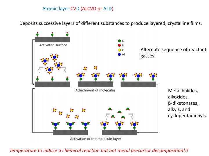
Atomic-layer CVD (ALCVD or ALD) Deposits successive layers of different substances to produce layered, crystalline films. Alternate sequence of reactant gasses Metal halides, alkoxides, -diketonates, alkyls, and cyclopentadienyls Temperature to induce a chemical reaction but not metal precursor decomposition!!!
Atomic-layer CVD (ALCVD) Advantages: Very high film quality Wide range of materials Thickness control on atomic scale Superior processability Disadvantages: Very slow: 0.01 nm/s Costs of precursors Waste of precursors in gas feed Limeted temperature windows
Atomic-layer CVD (ALCVD) Inorganics, 2018, 6, 34.
Atomic-layer CVD (ALCVD) Inorganics, 2018, 6, 34.
Atomic-layer CVD (ALCVD) Exposure times can be very long. The diffusion length must be kept short. This can be accomplished by forming the powders into thin wafers, rather than having a freestanding bed of powder. Increasing the pressure of the precursor also can significantly decrease the required exposure time. In some cases, the development of new, highly volatile precursors may be necessary.
Atomic-layer CVD (ALCVD) After the exposure step, excess precursor molecules and byproducts from the substrate must be removed by purging. This can be the longest step in the ALD cycle. In order to increase the production rate of wafers in the semiconductor industry, flow ALD systems with He as the carrier gas are used to flush gas-phase and physisorbed molecules from the sample. This is not trivial for a porous sample, since the excess precursor molecules and byproducts in the pores must diffuse to the to the exterior of the pore while in the presence of the carrier gas molecules.
Atomic-layer CVD (ALCVD) Obviously, when the purging step is incomplete, physisorbed precursor molecules may remain within the pore. Introducing the next reactant will lead to the reaction of these condensed species. (1) the formation of non-uniform films; (2) the formation of porous films; (3) the production of films that are much thicker than would be expected for ALD. The reaction of condensed films has been invoked as an explanation for the thick porous films formed by ALD procedures in SOFC electrodes.
")
")
")
")
")
")
")