Limits of Nb3Sn Strand Jc Enhancement


What are the Limits of
J
c
in Nb
3
Sn Strands?
The Ohio State University
The Ohio State University
M. D. Sumption
X. Xu
E. W. Collings
Hyper Tech
Hyper Tech
Research
Research
, Inc.
, Inc.
X. Peng
This work was supported by the U.S.
Department of Energy, High Energy Physics
university Grant No. DE-FG02-95ER40900
(OSU), DE-SC0010312 & DE-SC0011721 (OSU)
(University Program)


Low Temperature Superconductor
Workshop
Feb 16-18, 2015
Napa Valley, 2015
So, has the
J
c
of Nb
3
Sn reached its limit?
Before 2003, the non-Cu
J
c
of Nb
3
Sn
strands had been improved
continuously, mostly driven by
optimizing the Nb/Cu/Sn ratio, using
the right sort and amount of additions,
and proper heat treatments.
The improvement in
J
c
of Nb
3
Sn strands
has been flat last 10 years. The state-
of-the-art Nb
3
Sn strands achieve a 4.2
K, 12 T non-Cu
J
c
of ~3000-3500 A/mm
2
,
and a 15 T value of ~1600 A/mm
2
.
The development of
J
c
of Nb
3
Sn strands:
The non-Cu
J
c
of Nb
3
Sn strands depends on three parameters:
What’s the ideal grain size for
J
c
:
(Dietderich’s
thin film
experiment)
Several attempts to improve pinning capacity
A
Motowidlo et al., IEEE Trans. Appl. Supercon.
19
, 2568 (2009)
b
R. Durval
The internal oxidation method
First, “Internal oxidation”: oxygen diffuses in an A-B alloy, and selectively oxidizes the solute B.
Requirement: B is less noble than A.
As Nb-Zr is oxidized, f
ine ZrO
2
particles are formed.
Used in Nb
3
Sn films to
refine grain size
in 1960s.
Pre-dissolve O in Nb-Zr alloy?
SnO
2
powder as oxygen source?
B. A. Zeitlin et al., IEEE Trans. Appl. Supercon.
15
, 3393 (2005)
How to realize this in Nb
3
Sn films:
How to realize this in
Nb
3
Sn strands?
B. Zeitlin, 2001-2007
L. E. Rumaner et al., Metall. Mater. Trans. A
25
, 213 (1994)
Oxygen hardens metals,
making process hard.
Key point of this method:
Oxygen must already
dissolve in Nb-Zr before Nb-
Zr reacts with Sn.
Why no grain refinement in Zeitlin’s wire?
Zeitlin’s MEIT wire:
1. The “inert” Cu layer blocks
the path of oxygen transfer.
2. The diffusion of oxygen in Cu layer:
Assuming C
O
(O)=C
s
, C
O
(Nb1Zr)=0:
The O amount supplied is far from sufficient.
Can the (external) internal oxidation method work for Nb
3
Sn wires?
X. Xu et al., Appl. Phys. lett.
104
, 082602 (2014)
During heat
treatment:
Pure Ar
atmosphere:
no oxygen
supply
Ar-O mixture:
sufficient O
supply
T
c
of Nb drops by 0.93 K for 1 at.% O.
An experimental wire for (internal) internal oxidation
For control, we also made an analog with NbO
2
powder, which
cannot supply oxygen.
SnO2-625 °C/800 h
SnO2-625 °C/800 h
A tube type mono-filament:
What if we
tweak HT?
Layer
J
c
of Internal oxidation strands
Transport obtained 10.5 kA/mm2 at 10 T for SnO2-650x400h, (quench )
1.
Magnetization vs. field (M-B) loops were measured using a VSM at 4.2 K.
2.
A15 layer outer and inner diameters determination.
1, use the BSE image to
calculate
d
o
of FG A15
layer.
2, use the fracture SEM to
calculate the FG layer
thickness,
l
.
3, Calculate
d
i
=d
o
-2l
.
images from different places, 6
lines on each, then average:
80 nm
?
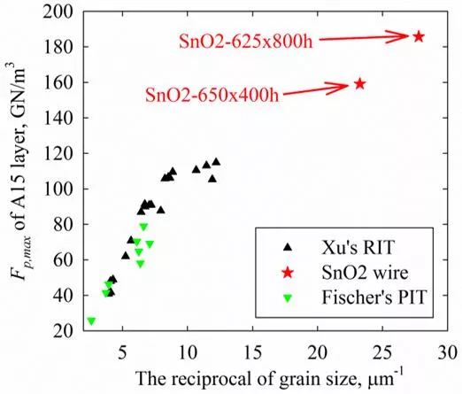
What’s the functional Form of Fpmax vs inverse grain size??
B
irr
was obtained by fitting the
F
p
-
B
curve
using
F
p
=Kb
p
(1-b)
q
, where b=B/
B
irr
.
F
p
-B
curves of Internal oxidation strands
Further improvements:
1. Ti additions =>
B
irr
↑
2. Higher Zr contents =>
smaller grain sizes?
For SnO2-625x800h, two
causes for increase in 12 T Jc:
1.
Increase in
F
p,max
.
2.
Some shift of Fp-B peaks.
What can we do to further improve the
J
c
:
2. Further refinement of grain size:
The Nb-1Zr & SnO
2
wire has a large
diameter (0.22 mm) and is under-reacted
after 800 h at 625 °C: if the subelement is
processed down and fully reacted, the
B
irr
should be improved by several tesla.
If we refine the grain size to 25 nm,
the
F
p
-
B
curve will peak at: 0.5
B
irr
.
If we refine the grain size to 25 nm,
the
F
p,max
will be: ~250 GN/m
3
.
So, how can we refine the
grain size down to 25 nm?
Use Nb-Zr alloy with
higher Zr content (e.g.,
1.5%) to to produce a
greater density of ZrO
2
particles.
Use a lower reaction
temperature (e.g., 605
°C).
Use other solid solution
alloys
1.
Increase in
B
irr
:
The Nb-1Zr & SnO
2
wire is based on binary Nb
3
Sn
phase:
B
irr
can be improved by Ta or Ti addition.
B
irr
increases with reaction time,
and plateaus when fully reacted.
F
p
-
B
curves for five different cases:
What if we can further optimize the internal oxidation strand, by both improving its
B
irr
and further reducing its grain size?
Engineering
J
c
and
I
c
for the five different cases:
Note: Assuming all the five cases have the same Nb
3
Sn area fraction with the state-of-the-art RRP strands:
the Nb
3
Sn area fraction in a subelement is 60%,
the non-Cu area fraction in a strand is 0.53,
the wire diameter is 0.8 mm.
What are the limits of
J
c
in Nb
3
Sn?
Maybe these ……
Lets put this on Peter Lee’s plot, and compare to YBCO and over-pressure processed
Bi:2212 wires
Conclusion
•
Grain size of 35 nm (as compared to 90-100 nm) has been
demonstrated
•
Layer
J
c
s of 9600 A/mm
2
at 12 T, 4.2 K, and 3800 A/mm
2
(extrapolated) at 15 T, 4.2 K have been seen
•
F
pmax
of 180 GN/m
3
has been shown (previous max was 90
GN/m
3
), with peak shift from 0.2
B
irr
-> 0.34
B
irr
•
Fill factors are low– must be demonstrated in conductor with
good fill factor – some ideas in development
More important than this specific approach:
•
F
p,max
vs grain sizes does not saturate below 90 nm!
•
It is possible to get fine grains in wires!
Assertions and Questions
•
Pushing grain sizes down to 25 nm might (should) push
the peak of the
F
p
curve to 0.5
B
irr
,
should give
F
p,max
= 250
GN/m
3
•
Such grain sizes seem possible, but may require the use of
non-commercial alloys
•
If a
J
e
of 1000 A/mm
2
is the criterion for use in a magnet,
and conductors with A15 fractions the same as present
day RRP could be made …
•
Could Nb
3
Sn could be used in magnets of 18 or even 23 T?
•
Can this be realized in a practical conductor?
•
If it can, it should be very important for HEP
Development of Nb3Sn strands has focused on optimizing Nb/Cu/Sn ratio, heat treatments, and grain size to improve critical current density (Jc). Despite advancements, recent progress in enhancing Jc has been limited. Various methods have been explored to increase pinning capacity, such as lower reaction temperatures, introducing alloy particles, and internal oxidation. Challenges remain in achieving optimal grain size and maximizing Jc performance.

Download Presentation

Please find below an Image/Link to download the presentation.
The content on the website is provided AS IS for your information and personal use only. It may not be sold, licensed, or shared on other websites without obtaining consent from the author. Download presentation by click this link. If you encounter any issues during the download, it is possible that the publisher has removed the file from their server.
E N D
Presentation Transcript
1 What are the Limits of Jcin Nb3Sn Strands? The Ohio State University M. D. Sumption X. Xu E. W. Collings Hyper Tech Research, Inc. X. Peng Low Temperature Superconductor Workshop Feb 16-18, 2015 Napa Valley, 2015 This work was supported by the U.S. Department of Energy, High Energy Physics university Grant No. DE-FG02-95ER40900 (OSU), DE-SC0010312 & DE-SC0011721 (OSU) (University Program)
The development of Jc of Nb3Sn strands: Before 2003, the non-Cu Jc of Nb3Sn strands had been improved continuously, mostly driven by optimizing the Nb/Cu/Sn ratio, using the right sort and amount of additions, and proper heat treatments. The improvement in Jc of Nb3Sn strands has been flat last 10 years. The state- of-the-art Nb3Sn strands achieve a 4.2 K, 12 T non-Cu Jc of ~3000-3500 A/mm2, and a 15 T value of ~1600 A/mm2. What s the ideal grain size for Jc: 50-100 nm 15-30 nm So, has the Jc of Nb3Sn reached its limit? The non-Cu Jc of Nb3Sn strands depends on three parameters: Birr, T (4.2 K) 23-26 27-28 Modest Nb3Sn fraction in subelements 60% 62-65% Little Grain size, nm 100-150 15-30 Huge! State-of-the-art RRP Limits/Optimal level Potentials for improving Jc (Dietderich s thin film experiment)
3 Several attempts to improve pinning capacity Methods Effect Problems Lower reaction temperature (<625 C) From 650 to 615 C, d is refined from 110 to 90 nm reaction time , Sn content Introducing Y or Gd particles by using Nb- Y or Nb-Gd alloy a At 750 C, 0.75 % Y refines grain size from 400-500 nm to 200-300 nm Y or Gd particles harden Nb alloy, and Nb- Y or Nb-Gd alloy is not commercially available Introducing nanometric Cu-Sn APCs b It is claimed that Fp,max was shifted to 0.5Birr. During heat treatment the Cu-Sn APCs agglomerate, reducing effectiveness 12 T layer Jc was around 1000 A/mm2. A Motowidlo et al., IEEE Trans. Appl. Supercon. 19, 2568 (2009) b R. Durval
4 The internal oxidation method First, Internal oxidation : oxygen diffuses in an A-B alloy, and selectively oxidizes the solute B. Requirement: B is less noble than A. As Nb-Zr is oxidized, fine ZrO2 particles are formed. Used in Nb3Sn films to refine grain size in 1960s. How to realize this in Nb3Sn strands? B. Zeitlin, 2001-2007 dissolve in Nb-Zr before Nb- Zr reacts with Sn. Key point of this method: Oxygen must already SnO2 powder as oxygen source? Cu matrix Barrier Nb1Zr fila Pre-dissolve O in Nb-Zr alloy? How to realize this in Nb3Sn films: Cu Nb-1at.%Zr foil Sn+SnO2 powders Anodization to form Nb2O5 Annealing at 1000 C to decompose Nb2O5 Oxygen hardens metals, making process hard. Sn coating Reaction at 1050 C L. E. Rumaner et al., Metall. Mater. Trans. A 25, 213 (1994) B. A. Zeitlin et al., IEEE Trans. Appl. Supercon. 15, 3393 (2005)
5 Why no grain refinement in Zeitlin s wire? Zeitlin s MEIT wire: 1. The inert Cu layer blocks the path of oxygen transfer. Cu matrix Barrier Nb-Zr fila Cu Sn+SnO2 powders 2. The diffusion of oxygen in Cu layer: Assuming CO(O)=Cs, CO(Nb1Zr)=0: T, 600 C D, m2/s Cs, at.% O in Cu 100 10-5 O in Nb 0.6 3 The O amount supplied is far from sufficient.
6 Can the (external) internal oxidation method work for Nb3Sn wires? During heat treatment: Cu matrix Pure Ar atmosphere: no oxygen supply Nb1 at.%Zr Cu Sn core Ar-O mixture: sufficient O supply Tc of Nb drops by 0.93 K for 1 at.% O. Reacted in pure Ar Intra-granular ZrO2 particles Inter-granular ZrO2 particles Reacted in Ar-O X. Xu et al., Appl. Phys. lett. 104, 082602 (2014)
7 An experimental wire for (internal) internal oxidation For control, we also made an analog with NbO2 powder, which cannot supply oxygen. A tube type mono-filament: SnO2 NbO2 Both: 650 C/150 h 200 nm 200 nm SnO2-625 C/800 h SnO2-625 C/800 h Ave: 36 nm What if we tweak HT?
8 Layer Jc of Internal oxidation strands Transport obtained 10.5 kA/mm2 at 10 T for SnO2-650x400h, (quench ) 1. 2. Magnetization vs. field (M-B) loops were measured using a VSM at 4.2 K. A15 layer outer and inner diameters determination. 1, use the BSE image to calculate do of FG A15 layer. images from different places, 6 lines on each, then average: # l, um 1 10.312 1 2 9.453 2 9.126 2 8.077 2 3 11.401 3 9.15 3 4 9.322 4 8.479 4 9.321 4 8.571 4 8.233 5 9.077 5 8.798 5 8.963 5 9.501 5 8.619 6 7.173 6 9.262 6 9.315 6 9.712 6 9.056 # l, um # l, um # l, um # l, um 8.68 1 8.132 1 6.356 1 7.72 2, use the fracture SEM to calculate the FG layer thickness, l. 5.44 2 7.952 9.38 3 7.436 3 7.605 3, Calculate di=do-2l.
9 What s the functional Form of Fpmax vs inverse grain size?? 80 nm ? 50-100 nm 15-30 nm
10 Fp-B curves of Internal oxidation strands For SnO2-625x800h, two causes for increase in 12 T Jc: 1. Increase in Fp,max. 2. Some shift of Fp-B peaks. Birr was obtained by fitting the Fp-B curve using Fp=Kbp(1-b)q, where b=B/Birr. Fp-B peak Grain size, nm Birr, T NbO2 - 625 C SnO2 - 650 C SnO2 - 625 C 0.22Birr 20.9 ~90 0.26Birr 23 45 0.34Birr ~20 36 Further improvements: 1. Ti additions => Birr 2. Higher Zr contents => smaller grain sizes?
1. Increase in Birr: The Nb-1Zr & SnO2 wire is based on binary Nb3Sn phase: Birr can be improved by Ta or Ti addition. What can we do to further improve the Jc: Grain size, Birr, T Fp-B peak nm SnO2 - 625 C Goal 0.34Birr ~20 36 0.5Birr 25 15 - 30 The Nb-1Zr & SnO2 wire has a large diameter (0.22 mm) and is under-reacted after 800 h at 625 C: if the subelement is processed down and fully reacted, the Birr should be improved by several tesla. Birr increases with reaction time, and plateaus when fully reacted. 2. Further refinement of grain size: If we refine the grain size to 25 nm, the Fp-B curve will peak at: 0.5Birr. If we refine the grain size to 25 nm, the Fp,max will be: ~250 GN/m3. So, how can we refine the grain size down to 25 nm? Use Nb-Zr alloy with higher Zr content (e.g., 1.5%) to to produce a greater density of ZrO2 particles. Use a lower reaction temperature (e.g., 605 C). Use other solid solution alloys 50-100 nm 15-30 nm
What if we can further optimize the internal oxidation strand, by both improving its Birr and further reducing its grain size? Fp-B curves for five different cases: 250 200 Fp = layer Jc * B, GN/m3 Improve Birr and refine grain size 150 Only Refine grain size to 25 nm Only Improve Birr to 25 T 100 Our SnO2 wire - 625 C/800h 50 Best RRP wire at present 0 12 0 5 10 15 20 25 Magnetic field, B, T Birr=25 T, Fp,max= 90 GN/m3, Fp-B peaks at 0.2Birr Birr=20 T, Fp,max=180 GN/m3, Fp-B peaks at 0.34Birr Birr=25 T, Fp,max=180 GN/m3, Fp-B peaks at 0.34Birr Birr=20 T, Fp,max=250 GN/m3, Fp-B peaks at 0.5Birr Birr=25 T, Fp,max=250 GN/m3, Fp-B peaks at 0.5Birr
What are the limits of Jc in Nb3Sn? Maybe these Engineering Jc and Icfor the five different cases: I. Present state-of-the- art RRP strands 100 - 120 0.2Birr ~90 25 5,000 3,000 1,600 800 2,700 1,600 850 430 II. The wire with SnO2 - 625 C / 800h 36 0.34Birr 180 20 9,600 5,760 3,050 1,530 3,800 2,280 1,210 610 III. Only improve Birr to 25 T by Ti doping, etc. 36 0.34Birr 180 25 16,400 9,840 5,200 2,620 7,800 4,680 2,480 1,250 IV. Only refine the grain size to 25 nm 25 0.5Birr ~250 20 20,000 12,000 6,360 3,200 12,500 7,500 4,000 2,000 V. Both improve the Birr to 25 T and refine the grain size down to 25 nm 25 0.5Birr ~250 25 20,800 12,480 6,600 3,320 16,000 9,600 5,100 2,560 Grain size, nm Fp-B peak Fp,max, GN/m3 Birr, T Layer Jc, A/mm2 Non-Cu Jc, A/mm2 Engineering Jc, A/mm2 Ic, A Layer Jc, A/mm2 Non-Cu Jc, A/mm2 Engineering Jc, A/mm2 Ic, A 12 T 15 T Note: Assuming all the five cases have the same Nb3Sn area fraction with the state-of-the-art RRP strands: the Nb3Sn area fraction in a subelement is 60%, the non-Cu area fraction in a strand is 0.53, the wire diameter is 0.8 mm.
Lets put this on Peter Lees plot, and compare to YBCO and over-pressure processed Bi:2212 wires
Conclusion Grain size of 35 nm (as compared to 90-100 nm) has been demonstrated Layer Jcs of 9600 A/mm2 at 12 T, 4.2 K, and 3800 A/mm2 (extrapolated) at 15 T, 4.2 K have been seen Fpmax of 180 GN/m3 has been shown (previous max was 90 GN/m3), with peak shift from 0.2Birr -> 0.34 Birr Fill factors are low must be demonstrated in conductor with good fill factor some ideas in development More important than this specific approach: Fp,max vs grain sizes does not saturate below 90 nm! It is possible to get fine grains in wires!
Assertions and Questions Pushing grain sizes down to 25 nm might (should) push the peak of the Fp curve to 0.5 Birr, should give Fp,max = 250 GN/m3 Such grain sizes seem possible, but may require the use of non-commercial alloys If a Jeof 1000 A/mm2 is the criterion for use in a magnet, and conductors with A15 fractions the same as present day RRP could be made Could Nb3Sn could be used in magnets of 18 or even 23 T? Can this be realized in a practical conductor? If it can, it should be very important for HEP