Iron Deficiency Anemia (IDA) Overview
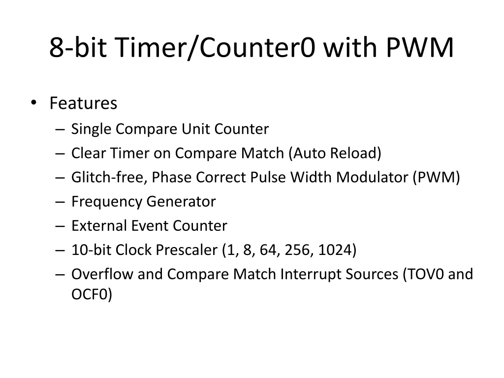

8-bit Timer/Counter0 with PWM
•
Features
–
Single Compare Unit Counter
–
Clear Timer on Compare Match (Auto Reload)
–
Glitch-free, Phase Correct Pulse Width Modulator (PWM)
–
Frequency Generator
–
External Event Counter
–
10-bit Clock Prescaler (1, 8, 64, 256, 1024)
–
Overflow and Compare Match Interrupt Sources (TOV0 and
OCF0)

Registers
•
The Timer/Counter (TCNT0) and Output Compare
Register (OCR0) are 8-bit registers.
•
Interrupt request (abbreviated to Int.Req. in the
figure) signals are all visible in the Timer Interrupt
Flag Register (TIFR).
•
All interrupts are individually masked with the Timer
Interrupt Mask Register (TIMSK).
•
TIFR and TIMSK are not shown in the figure since
these registers are shared by other timer units.
Registers (lanj.)
•
The Timer/Counter can be clocked internally, via the
prescaler, or by an external clock source on the T0
pin.
•
The Clock Select logic block controls which clock
source and edge the Timer/Counter uses to
increment (or decrement) its value.
•
The Timer/Counter is inactive when no clock source
is selected.
•
The output from the Clock Select logic is referred to
as the timer clock (clkT0).
Registers (lanj.)
•
The double buffered Output Compare Register
(OCR0) is compared with the Timer/Counter value at
all times.
•
The result of the compare can be used by the
waveform generator to generate a PWM or variable
frequency output on the Output Compare Pin (OC0).
•
The compare match event will also set the Compare
Flag (OCF0) which can be used to generate an output
compare interrupt request.
Registers (lanj.)
•
TCCR0 – Timer/Counter Control Register
•
TCNT0 – Timer/Counter Register
•
OCR0 – Output Compare Register
•
TIMSK – Timer/Counter Interrupt Mask
Register
•
TIFR – Timer/Counter Interrupt Flag Register
Mode Timer/Counter 0
•
Normal
•
CTC (Clear Timer on Compare Match)
•
Fast PWM (Single Slope PWM)
•
Phase Correct PWM (Double Slope PWM)
TCCR0 – Timer/Counter Control
Register
Bit 7 – FOC0: Force Output Compare
•
The FOC0 bit is only active when the WGM00 bit specifies a
non-PWM mode.
–
However, for ensuring compatibility with future devices, this bit must
be set to zero when TCCR0 is written when operating in PWM mode.
•
When writing a logical one to the FOC0 bit, an immediate
compare match is forced on the Waveform Generation unit.
•
The OC0 output is changed according to its COM01:0 bits
setting. Note that the FOC0 bit is implemented as a strobe.
–
Therefore it is the value present in the COM01:0 bits that determines
the effect of the forced compare.
•
A FOC0 strobe will not generate any interrupt, nor will it clear
the timer in CTC mode using OCR0 as TOP.
•
The FOC0 bit is always read as zero.
Bit 3, 6 – WGM0[1:0]: Waveform
Generation Mode
Bit 5:4 – COM01:0: Compare Match
Output Mode
•
Pin OC0 pada mode non-PWM
•
Pin OC0 pada mode Fast PWM
•
Pin OC0 pada mode Phase Correct PWM
Bit 2:0 – CS02:0: Clock Select
•
Timer
Clock
= {Off, fc
, f
c
/8, f
c
/64, f
c
/256, f
c
/1024}
TIMSK – Timer/Counter Interrupt
Mask Register
TIFR – Timer/Counter Interrupt Flag
Register
Normal Mode
•
The simplest mode of operation is the normal
mode (WGM01:0 = 0).
•
In this mode the counting direction is always
up (incrementing), and no counter clear is
performed.
•
The counter simply overruns when it passes
its maximum 8-bit value (TOP = 0xFF) and then
restarts from the bottom (0x00).
Normal Mode (lanj.)
•
In normal operation the Timer/Counter Overflow
Flag (TOV0) will be set in the same timer clock cycle
as the TCNT0 becomes zero.
•
The TOV0 Flag in this case behaves like a ninth bit,
except that it is only set, not cleared.
•
However, combined with the timer overflow
interrupt that automatically clears the TOV0 Flag, the
timer resolution can be increased by software.
Normal Mode (lanj.)
•
There are no special cases to consider in the
normal mode, a new counter value can be
written anytime.
•
The output compare unit can be used to
generate interrupts at some given time.
–
Using the output compare to generate waveforms
in Normal mode is not recommended, since this
will occupy too much of the CPU time.
Clear Timer on Compare Match (CTC)
Mode
•
In Clear Timer on Compare or CTC mode
(WGM01:0 = 2), the OCR0 Register is used to
manipulate the counter resolution.
•
In CTC mode the counter is cleared to zero
when the counter value (TCNT0) matches the
OCR0.
CTC Mode (lanj.)
•
The OCR0 defines the top value for the
counter, hence also its resolution.
•
This mode allows greater control of the
compare match output frequency.
•
It also simplifies the operation of counting
external events.
CTC Mode (lanj.)
•
The timing diagram for the CTC mode is
shown in Figure 14-5.
•
The counter value (TCNT0) increases until a
compare match occurs between TCNT0 and
OCR0, and then counter (TCNT0) is cleared.
Waktu/Frekuensi Mode CTC
•
N = {1, 8, 64, 256, 1024}Fast PWM Mode
•
The fast Pulse Width Modulation or fast PWM
mode (WGM01:0 = 3) provides a high
frequency PWM waveform generation option.
•
The fast PWM differs from the other PWM
option by its single-slope operation.
•
The counter counts from BOTTOM to MAX
then restarts from BOTTOM.
Fast PWM Mode (lanj.)
•
In non-inverting Compare Output mode, the Output
Compare (OC0) is cleared on the compare match
between TCNT0 and OCR0, and set at BOTTOM.
•
In inverting Compare Output mode, the output is set
on compare match and cleared at BOTTOM.
•
Due to the single-slope operation, the operating
frequency of the fast PWM mode can be twice as
high as the phase correct PWM mode that use dual-
slope operation.
Fast PWM Mode (lanj.)
•
This high frequency makes the fast PWM mode well
suited
•
for power regulation, rectification, and DAC
applications.
•
High frequency allows physically small sized external
components (coils, capacitors), and therefore
reduces total system cost.
Fast PWM Mode (lanj.)
•
In fast PWM mode, the counter is
incremented until the counter value matches
the MAX value.
•
The counter is then cleared at the following
timer clock cycle.
•
The timing diagram for the fast PWM mode is
shown in Figure 14-6.
Fast PWM Mode (lanj.)
•
The TCNT0 value is in the timing diagram
shown as a histogram for illustrating the
single-slope operation.
•
The diagram includes non-inverted and
inverted PWM outputs.
–
The small horizontal line marks on the TCNT0
slopes represent compare matches between OCR0
and TCNT0.
Phase Correct PWM Mode
•
The phase correct PWM mode (WGM01:0 = 1)
provides a high resolution phase correct PWM
waveform generation option.
•
The phase correct PWM mode is based on a
dual-slope operation.
•
The counter counts repeatedly from BOTTOM
to MAX and then from MAX to BOTTOM.
Phase Correct PWM Mode (lanj.)
•
In non-inverting Compare Output mode, the Output
Compare (OC0) is cleared on the compare match
between TCNT0 and OCR0 while up-counting, and
set on the compare match while down-counting.
•
In inverting Output Compare mode, the operation is
inverted.
•
The dual-slope operation has lower maximum
operation frequency than single slope operation.
Phase Correct PWM Mode (lanj.)
•
However, due to the symmetric feature of the
dual-slope PWM modes, these modes are
preferred for motor control applications.
•
The PWM resolution for the phase correct
PWM mode is fixed to eight bits.
•
In phase correct PWM mode the counter is
incremented until the counter value matches
MAX.
Phase Correct PWM Mode (lanj.)
•
When the counter reaches MAX, it changes
the count direction.
•
The TCNT0 value will be equal to MAX for one
timer clock cycle.
•
The timing diagram for the phase correct
PWM mode is shown on Figure 14-7.
Phase Correct PWM Mode (lanj.)
•
The TCNT0 value is in the timing diagram
shown as a histogram for illustrating the dual-
slope operation.
•
The diagram includes non-inverted and
inverted PWM outputs.
•
The small horizontal line marks on the TCNT0
slopes represent compare matches between
OCR0 and TCNT0.
Frekuensi Mode PCPWM
•
N = {1, 8, 64, 256, 1024}Iron Deficiency Anemia (IDA) is a common condition characterized by low iron levels, affecting both developed and developing countries. Learn about the background, definition, epidemiology, and key laboratory findings for diagnosing IDA.

Uploaded on Feb 20, 2025 | 0 Views
Download Presentation

Please find below an Image/Link to download the presentation.
The content on the website is provided AS IS for your information and personal use only. It may not be sold, licensed, or shared on other websites without obtaining consent from the author.If you encounter any issues during the download, it is possible that the publisher has removed the file from their server.
You are allowed to download the files provided on this website for personal or commercial use, subject to the condition that they are used lawfully. All files are the property of their respective owners.
The content on the website is provided AS IS for your information and personal use only. It may not be sold, licensed, or shared on other websites without obtaining consent from the author.
E N D
Presentation Transcript
8-bit Timer/Counter0 with PWM Features Single Compare Unit Counter Clear Timer on Compare Match (Auto Reload) Glitch-free, Phase Correct Pulse Width Modulator (PWM) Frequency Generator External Event Counter 10-bit Clock Prescaler (1, 8, 64, 256, 1024) Overflow and Compare Match Interrupt Sources (TOV0 and OCF0)
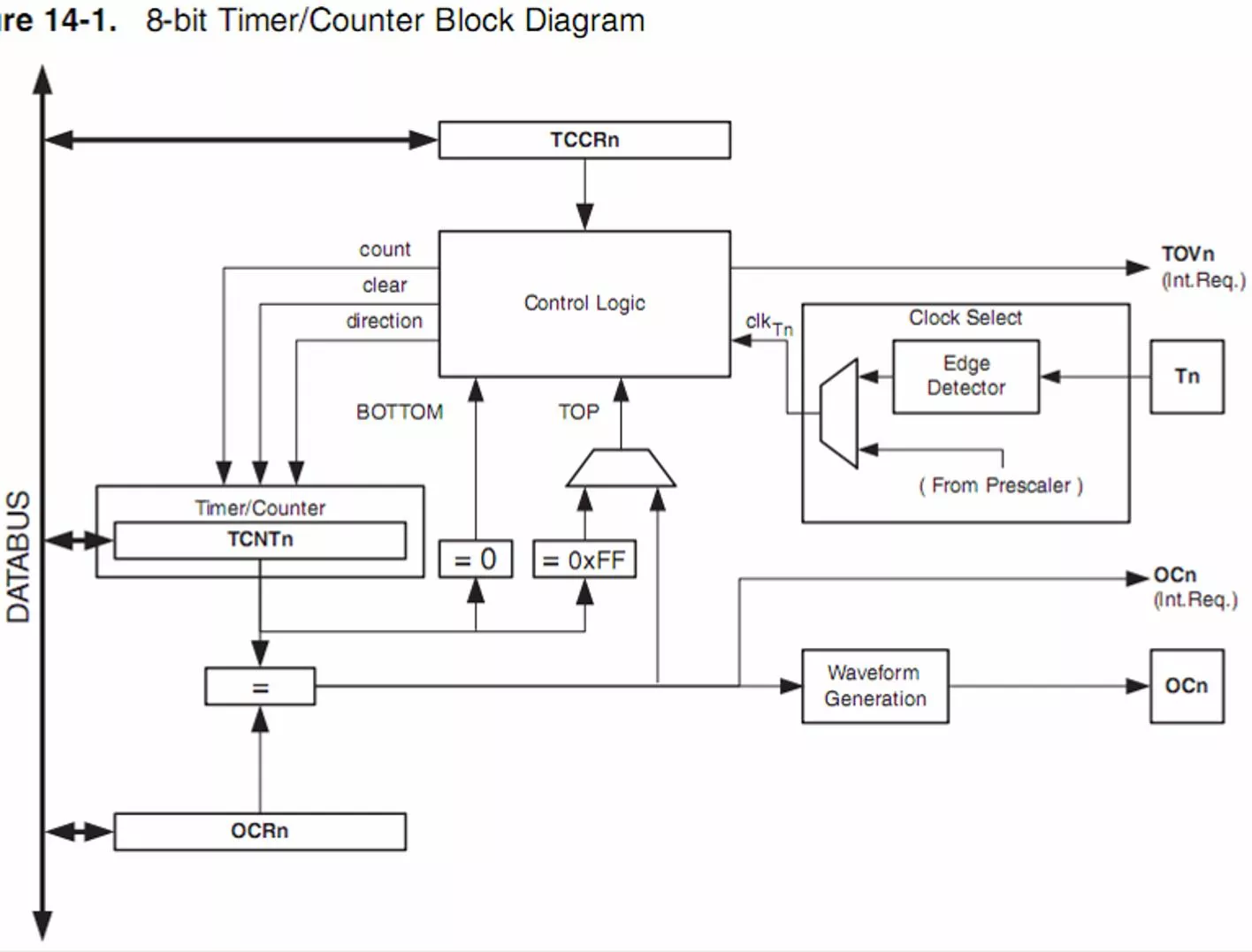
Registers The Timer/Counter (TCNT0) and Output Compare Register (OCR0) are 8-bit registers. Interrupt request (abbreviated to Int.Req. in the figure) signals are all visible in the Timer Interrupt Flag Register (TIFR). All interrupts are individually masked with the Timer Interrupt Mask Register (TIMSK). TIFR and TIMSK are not shown in the figure since these registers are shared by other timer units.
Registers (lanj.) The Timer/Counter can be clocked internally, via the prescaler, or by an external clock source on the T0 pin. The Clock Select logic block controls which clock source and edge the Timer/Counter uses to increment (or decrement) its value. The Timer/Counter is inactive when no clock source is selected. The output from the Clock Select logic is referred to as the timer clock (clkT0).
Registers (lanj.) The double buffered Output Compare Register (OCR0) is compared with the Timer/Counter value at all times. The result of the compare can be used by the waveform generator to generate a PWM or variable frequency output on the Output Compare Pin (OC0). The compare match event will also set the Compare Flag (OCF0) which can be used to generate an output compare interrupt request.
Registers (lanj.) TCCR0 Timer/Counter Control Register TCNT0 Timer/Counter Register OCR0 Output Compare Register TIMSK Timer/Counter Interrupt Mask Register TIFR Timer/Counter Interrupt Flag Register
Mode Timer/Counter 0 Normal CTC (Clear Timer on Compare Match) Fast PWM (Single Slope PWM) Phase Correct PWM (Double Slope PWM)
TCCR0 Timer/Counter Control Register
Bit 7 FOC0: Force Output Compare The FOC0 bit is only active when the WGM00 bit specifies a non-PWM mode. However, for ensuring compatibility with future devices, this bit must be set to zero when TCCR0 is written when operating in PWM mode. When writing a logical one to the FOC0 bit, an immediate compare match is forced on the Waveform Generation unit. The OC0 output is changed according to its COM01:0 bits setting. Note that the FOC0 bit is implemented as a strobe. Therefore it is the value present in the COM01:0 bits that determines the effect of the forced compare. A FOC0 strobe will not generate any interrupt, nor will it clear the timer in CTC mode using OCR0 as TOP. The FOC0 bit is always read as zero.
Bit 3, 6 WGM0[1:0]: Waveform Generation Mode
Bit 5:4 COM01:0: Compare Match Output Mode Pin OC0 pada mode non-PWM
Bit 2:0 CS02:0: Clock Select TimerClock= {Off, fc, fc/8, fc/64, fc/256, fc/1024}
TIMSK Timer/Counter Interrupt Mask Register
TIFR Timer/Counter Interrupt Flag Register
Normal Mode The simplest mode of operation is the normal mode (WGM01:0 = 0). In this mode the counting direction is always up (incrementing), and no counter clear is performed. The counter simply overruns when it passes its maximum 8-bit value (TOP = 0xFF) and then restarts from the bottom (0x00).
Normal Mode (lanj.) In normal operation the Timer/Counter Overflow Flag (TOV0) will be set in the same timer clock cycle as the TCNT0 becomes zero. The TOV0 Flag in this case behaves like a ninth bit, except that it is only set, not cleared. However, combined with the timer overflow interrupt that automatically clears the TOV0 Flag, the timer resolution can be increased by software.
Normal Mode (lanj.) There are no special cases to consider in the normal mode, a new counter value can be written anytime. The output compare unit can be used to generate interrupts at some given time. Using the output compare to generate waveforms in Normal mode is not recommended, since this will occupy too much of the CPU time.
Clear Timer on Compare Match (CTC) Mode In Clear Timer on Compare or CTC mode (WGM01:0 = 2), the OCR0 Register is used to manipulate the counter resolution. In CTC mode the counter is cleared to zero when the counter value (TCNT0) matches the OCR0.
CTC Mode (lanj.) The OCR0 defines the top value for the counter, hence also its resolution. This mode allows greater control of the compare match output frequency. It also simplifies the operation of counting external events.
CTC Mode (lanj.) The timing diagram for the CTC mode is shown in Figure 14-5. The counter value (TCNT0) increases until a compare match occurs between TCNT0 and OCR0, and then counter (TCNT0) is cleared.
Waktu/Frekuensi Mode CTC N = {1, 8, 64, 256, 1024} ( ) + . 1 N OCRn = t OCn f clock f = clock + f ( ) OCn . 2 . 1 N OCRn
Fast PWM Mode The fast Pulse Width Modulation or fast PWM mode (WGM01:0 = 3) provides a high frequency PWM waveform generation option. The fast PWM differs from the other PWM option by its single-slope operation. The counter counts from BOTTOM to MAX then restarts from BOTTOM.
Fast PWM Mode (lanj.) In non-inverting Compare Output mode, the Output Compare (OC0) is cleared on the compare match between TCNT0 and OCR0, and set at BOTTOM. In inverting Compare Output mode, the output is set on compare match and cleared at BOTTOM. Due to the single-slope operation, the operating frequency of the fast PWM mode can be twice as high as the phase correct PWM mode that use dual- slope operation.
Fast PWM Mode (lanj.) This high frequency makes the fast PWM mode well suited for power regulation, rectification, and DAC applications. High frequency allows physically small sized external components (coils, capacitors), and therefore reduces total system cost.
Fast PWM Mode (lanj.) In fast PWM mode, the counter is incremented until the counter value matches the MAX value. The counter is then cleared at the following timer clock cycle. The timing diagram for the fast PWM mode is shown in Figure 14-6.
Fast PWM Mode (lanj.) The TCNT0 value is in the timing diagram shown as a histogram for illustrating the single-slope operation. The diagram includes non-inverted and inverted PWM outputs. The small horizontal line marks on the TCNT0 slopes represent compare matches between OCR0 and TCNT0.
f OCnPWM= clock f 256 . N
Phase Correct PWM Mode The phase correct PWM mode (WGM01:0 = 1) provides a high resolution phase correct PWM waveform generation option. The phase correct PWM mode is based on a dual-slope operation. The counter counts repeatedly from BOTTOM to MAX and then from MAX to BOTTOM.
Phase Correct PWM Mode (lanj.) In non-inverting Compare Output mode, the Output Compare (OC0) is cleared on the compare match between TCNT0 and OCR0 while up-counting, and set on the compare match while down-counting. In inverting Output Compare mode, the operation is inverted. The dual-slope operation has lower maximum operation frequency than single slope operation.
Phase Correct PWM Mode (lanj.) However, due to the symmetric feature of the dual-slope PWM modes, these modes are preferred for motor control applications. The PWM resolution for the phase correct PWM mode is fixed to eight bits. In phase correct PWM mode the counter is incremented until the counter value matches MAX.
Phase Correct PWM Mode (lanj.) When the counter reaches MAX, it changes the count direction. The TCNT0 value will be equal to MAX for one timer clock cycle. The timing diagram for the phase correct PWM mode is shown on Figure 14-7.
Phase Correct PWM Mode (lanj.) The TCNT0 value is in the timing diagram shown as a histogram for illustrating the dual- slope operation. The diagram includes non-inverted and inverted PWM outputs. The small horizontal line marks on the TCNT0 slopes represent compare matches between OCR0 and TCNT0.
f OCnPCPWM= clock f 512 . N
Frekuensi Mode PCPWM N = {1, 8, 64, 256, 1024} f OCnPCPWM= clock f 512 . N


")
")
")
")


")
")
")
")
")
")


")
")
")
")


")
")
")
")