Errors in Current Mirrors and BJTs Analysis
Explore the impact of matching errors in CMOS current mirrors and BJT devices, including examples and standard deviations. Delve into process parameters and matching errors affecting collector current in BJT devices.

Download Presentation

Please find below an Image/Link to download the presentation.
The content on the website is provided AS IS for your information and personal use only. It may not be sold, licensed, or shared on other websites without obtaining consent from the author. If you encounter any issues during the download, it is possible that the publisher has removed the file from their server.
You are allowed to download the files provided on this website for personal or commercial use, subject to the condition that they are used lawfully. All files are the property of their respective owners.
The content on the website is provided AS IS for your information and personal use only. It may not be sold, licensed, or shared on other websites without obtaining consent from the author.
E N D
Presentation Transcript
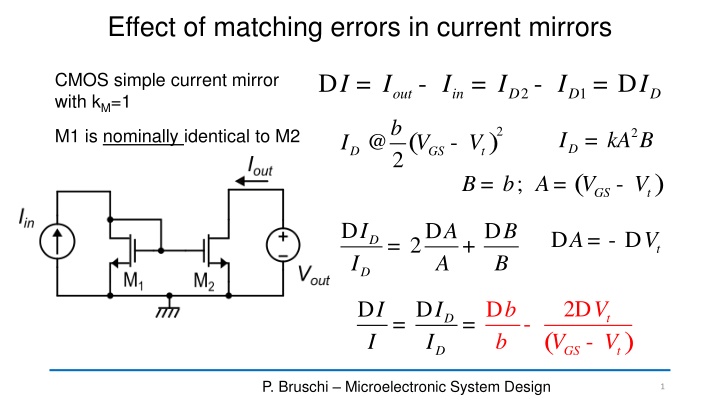
Effect of matching errors in current mirrors D = - = - = D I I I I I I CMOS simple current mirror with kM=1 2 1 out in D D D b 2 2 M1 is nominally identical to M2 ( ) = D I kA B @ - I V V D GS t 2 ( ) = ; = - B b A V V GS t D D D I A B D = - D A V = 2 + D t I A B D 2 D D D D V I I b = = - t D ( ) - I I b V V D GS t P. Bruschi Microelectronic System Design 1
Standard deviations 2 2 s D - V 2 D = + s s t D I b V V D GS t b I D C WL C b D= s b 2 D D D D V I I b b = = - t D ( ) - I I b V V D GS t V = s t V WL t P. Bruschi Microelectronic System Design 2
Examples C C WL V b D= = s s t b V WL t b 2 = 0.03 m 8.5 mV 2 C m s b D - V 2 D = + s s t D I b m C m = V V D tV GS t b I D 2 s Case 1: L=W=1 m VGS-Vt =100 mV D - V = 0.03 = 0.17 = 0.173 (17.3%) s s t D D b I V V D GS s t b I D 2 Case 1: L=W=1 m VGS-Vt =500 mV D - V = 0.03 = 0.034 = 0.0453 (4.53%) s s t D D b I V V D GS 2 t b I D s Case 1: L=W=10 m VGS-Vt =500 mV D - V = 0.003 = 0.0034 = 0.00453 (0.453%) s s t D D b I V V D GS t b I D P. Bruschi Microelectronic System Design 3
Matching in BJT: process parameters Q1 and Q2 are nominally identical and placed in the same chip. They are affected by matching errors Q1 and Q2 are biased with identical VCE>> VCESATand individual VBEvoltages such that Q1 and Q2 carry the same collector current amperometers I I V V V V BE V BE V = ln C V V = 1 + @ CB I I e I e t t BE T C S S S A The foundry provides (of the minimum size BJT) * BE e V D D I D D I I * D @ D = - S V V V D = - 0 C S V V I I I = D = BE BE T 1 2 C C C BE T D = 0 I I I I C S C S s generically - P. Bruschi Microelectronic System Design 4
Matching errors in BJT current mirrors V V V V BE V BE V = 1 + @ CB I I e I e t t C S S A D D I I = C S D = - I I I I I 2 1 C C C C S V V * D D D I I * = - D = - S S V V BE BE T I I S T S = 100 V - s 300 V s typical values: * BE e V - * BE D D V = = s s - D D I I V C S - 2 - 2 0.4 10 1.2 10 s = T s I I D I C S C * BE e V area D = s I - Note: C * BE D V P. Bruschi Microelectronic System Design 5