Electronics Systems Review Findings for CEPC Project
Explore the insightful comments from the IDRC review report on the electronics system for the CEPC project, highlighting key risks and strategies related to chip development, power schemes, and data transmission options.

Download Presentation

Please find below an Image/Link to download the presentation.
The content on the website is provided AS IS for your information and personal use only. It may not be sold, licensed, or shared on other websites without obtaining consent from the author. If you encounter any issues during the download, it is possible that the publisher has removed the file from their server.
You are allowed to download the files provided on this website for personal or commercial use, subject to the condition that they are used lawfully. All files are the property of their respective owners.
The content on the website is provided AS IS for your information and personal use only. It may not be sold, licensed, or shared on other websites without obtaining consent from the author.
E N D
Presentation Transcript
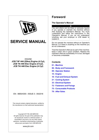
IDRC review report electronics system related Comments from IDRC Moving to a triggered readout scheme is listed as a backup plan, however it is unlikely that this would be viable once the project is well underway due to the impact on the FEE-ASIC designs as the backend is radically different. (related to R.2) By far the highest risk in the electronics is designing and delivering the 6 FEE-ASICs needed. For the 6 FEE-ASICs needed to readout the detector subsystems, there is significant effort needed. (related to R.1) There are design teams already working on 2 of the chips (for VTX and TPC detectors) and another has been identified for the ITK. Not exactly. Design teams are also assigned to OTK and SiPM (for ECAL+HCAL+Muon). Principle ASIC schemes & readout schemes were prepared. Due to the short of time in the review, not much details were discussed. Supplement materials can be prepared further. It is planned that most chips would share the same technology node (55 nm) and possibly share some blocks, which is very efficient but not so easy in practice. Agreed, but not exactly. Technology will be chosen based on the most suitable case. Some are unified, for OTK, SiPM, TaoTie, Chitu, KinWoo. Others are different, for VTK, BaSha. 1
IDRC review report electronics system related Comments from IDRC The FE-ASIC progress should be closely monitored by the electronics coordinators. . The timeline and development path should be clearly specified (number of intermediate prototypes, variants ) (related to R.1) The development of these common chips by a strong central group is a good choice. However, it s a heavy load and the manpower needed for full verification and testing should not be underestimated. The manpower absorbed by this common task may deprive other developments, in particular for the FE ASICs. If all the chips need to be developed in China (to be discussed with management), the resources are probably insufficient, especially if they are distributed over several labs. In any case a strong central facility (like CERN-MIC does for LHC) is essential. Otherwise look at existing chips and whether they could be adapted to CEPC. Agreed, and it is the idea. On the one hand, IHEP will be THE central facility to develop the ASIC, on the other hand, actually design power has been allocated to each FE ASIC (will be listed in the supplement file). We have also looked at existing chips. One candidate is the SiPM ASIC for CAL. However it is developed by a company (the leader formerly has the background of HEP), the cost is not possible for such a large facility of CEPC. Thus it also has to be design by ourselves. We also warmly welcome international collaborators for the joint effort of ASIC development 2
IDRC review report electronics system related Comments from IDRC The DC-DC converter is at an early stage. The GaN transistor has been selected, though needs testing for radiation tolerance. The switching frequency of the design is currently 5MHz, but the group is investigating moving to a higher frequency to improve the conversion efficiency. The converter circuitry itself is an established design. The parallel power scheme baseline plan is low risk, but serial powering has benefits if it can be used. The team should monitor developments elsewhere in case progress makes a serial scheme viable. Fully agreed. We will keep pace on R&D of the serial powering scheme. The wireless data transmission option is a backup plan, however it is not a low-risk backup. Significant R&D remains in miniaturizing and shielding, which is envisioned being driven by an industrial partner. . Use inside the detector for readout of, eg, the silicon system would also require development of shielding and significant testing of the level of noise pickup the transmitters might induce in the detector elements. However, the wireless readout development should not take resources from the baseline electronics effort. Agreed. The R&D resources will be independent from the baseline effort. 3
IDRC review report electronics system related Recommendations from IDRC R.1 Establish the timeline for all the FE ASICs development for all the sub-detectors and their state of maturity. R.2 Establish early enough the readout scheme (triggerless) so that no efforts are wasted on developments that will not be retained, chips unlikely to accommodate both R/O schemes. Agreed and it is almost established. We are waiting for the final report from the MDI background rate to finalized the electronics schemes. R.3 For the triggerless readout, show the maximum rates that can be handled, the safety margin that is included and what happens if the occupancy gets higher. What throttle scheme can be used? The maximum rate were currently calculated based on MDI effort, and were summarized in the table. In the supplement files, it can be seen that for most sub-detector, data link are at relatively low load of the data rate. At the meanwhile, only one fiber is used for each module while the maximum possibility is 4 fibers. The occupancy variations is already considered in FE-ASIC, as they are all zero-suppressed (or event-driven). The most/only risky part is VTX FE. As the current data rate is already 1~2Gbps per RSU. It is not sure if the cooling capability is enough for the current stitching scheme. We will keep eyes on it while the R&D is ongoing. Once it is proved to be problematic, fast trigger will be added to the VTX detector. 4
Status of FE & common ASIC Name Application Functional Maturity Comment Similar chips Common Elec Data Link 2~3 Key blocks ready, protocol TBD lpGBT ChiTu Common Elec Optical 3~4 Real module verified VTRx KinWoo Common Elec Data Aggregation 2 Although needs scheme, but a pure digital ASIC, low risk TaoTie GBTx HCC Common Elec DC-DC 2 Initial stage, but the scheme are conventional and low risk. GaN has been preliminarily verified. Inductors to be selected and tested for Magnet. BaSha bPolx FEAST VTX VTX-Stitching 2~3 Single chip fully verified. Will be focused on stitching issues ALICE-ITS3 Taichu TEPIX-TPC TPC Pixel TPC 3~4 TPC module to be beam-tested. Further optimization is ongoing Gridpix Timepix3 ITK-B ? ITK-E ? OTK-ROC OTK LGAD-TOF 2 With preliminary scheme, while TDC & similar FE is already tapedout and wait for test. Cd & power to be optimized for a real design. ALTIROC SiPM-ROC SiPMASIC ECAL, HCAL, Muon 2~3 Schemes verified in previous chips. No show stopper for all key blocks. Waiting for the detector finalization & device selection to start the design HGCROC SPIROC Maturity: 1 prototyped, further optimization required; 5 from scratch; 2: initial design proposed, R&D needed; 3: with experience or previous design, no show stopper; 4 verified for the real detector. 5
Timeline for all the FE ASICs - VTX 2025 Taichu debugging and finalization Stitching design on TJ180, based on Taichu s previous design, for low cost Bending chip electrical test based on Taichu3-most2, at single chip level. 2026 Taichu-Stitching-180 chip test TJ65 design kit finalization (expected) Taichu4 prototype design on TJ65 for process evaluation (MPW or combined-engineering), at single chip level 2027 Taichu-Stitching-180 mechanical prototype and test TJ65 chip prototype test. 2028~2029 TJ65-stitching based on previous experience of TJ180-stitching & TJ65 prototype Comment: Stitching on TJ65 currently is not cost-effective and high risk, given that the design kit is not finalized. Two parallel design to verify the final scheme: Stitching on TJ180; prototype on TJ65 6
Timeline for all the FE ASICs - TPC 2025 Beamtest with TPC module based on current TEPIX chip. Detector optimization for a final pixel size. 2026 Chip optimization with the final detector design Chip test 2027 Prototype with the final detector & final chip Beamtest with the final module 7
Timeline for all the FE ASICs SiPM FE for CAL & Muon 2024 Detector s final requirements to FE SiPM s final selection for FE design 2025 The first version of SiPM ASIC: with main analog performance and basic digital functionality Test & verification of the SiPM ASIC 1stwith main performance If mostly verified If critical issue found 2026 2027 Chip debugging & optimization (2ndMPW) 1stEngineering Prototype for the 7000chn HCAL 2026 Contact for existing chip (minor modification might needed); find for (international) collaboration 2027 7000chn HCAL prototype based on xxx chip Comment: Rough price of the existing chip is too high for a mass production prototype Self-R&D is necessary for the final CEPC ECAL 2026~2029 SiPM ASIC design with 2 MPW + 1~2 engineering run, aiming for real CEPC CAL 8
Timeline for all the FE ASICs - OTK For OTK prototype as the recent plan 2025 First chip prototype test for the FASTPMT ASIC (FPMROC) (from other project with similar requirement); Chip debugging & optimization 2026 FASTPMT ASIC finalization 2027 Co-test by FASTPMT ASIC with AC-LGAD sensor prototype For real CEPC OTK FE-ASIC 2025 Detector Cd and size optimization & finalization Specification and schemes review for OTK FE 2026~2029 OTK FE ASIC design with 2 MPW + 1~2 engineering run Comment: OTK detector R&D can be guaranteed by the previous & ongoing FASTPMT ASIC Real CEPC OTK needs detector finalization, which needs time Design power can be shifted in timeline between OTK & SiPM 9
Timeline for all the FE ASICs common ASIC 2025.6 2024.8 2024.9 2024.10 2024.12 2025.3 Overall Electronics system Sub-Det readout Elec scheme finalization Specification & background finalization Overall Electronics scheme finalization Elec TDR Draft1 Elec cost Draft1 2024.10 2024.11 2025.1 2025.3 2026.1 Irradiation test Power & DC- DC Module DC-DC module performance from simulation GaN Selection DC-DC BaSha module prototype 2027.6 DC-DC Controller schematic design 2024.8 2024.10 Data Link Specification finalization Protocol define ChiTu Chip prototype Ref-TDR release 10