Comprehensive Overview of Full Ceramic Grid Technology in Microfabrication
Explore the innovative full ceramic grid technology in microfabrication, including insights into the process flow, materials utilized, and applications. Learn about the components, layers, and bonding techniques involved in this advanced manufacturing method, offering high precision and thermal stability for various semiconductor devices.

Download Presentation

Please find below an Image/Link to download the presentation.
The content on the website is provided AS IS for your information and personal use only. It may not be sold, licensed, or shared on other websites without obtaining consent from the author.If you encounter any issues during the download, it is possible that the publisher has removed the file from their server.
You are allowed to download the files provided on this website for personal or commercial use, subject to the condition that they are used lawfully. All files are the property of their respective owners.
The content on the website is provided AS IS for your information and personal use only. It may not be sold, licensed, or shared on other websites without obtaining consent from the author.
E N D
Presentation Transcript
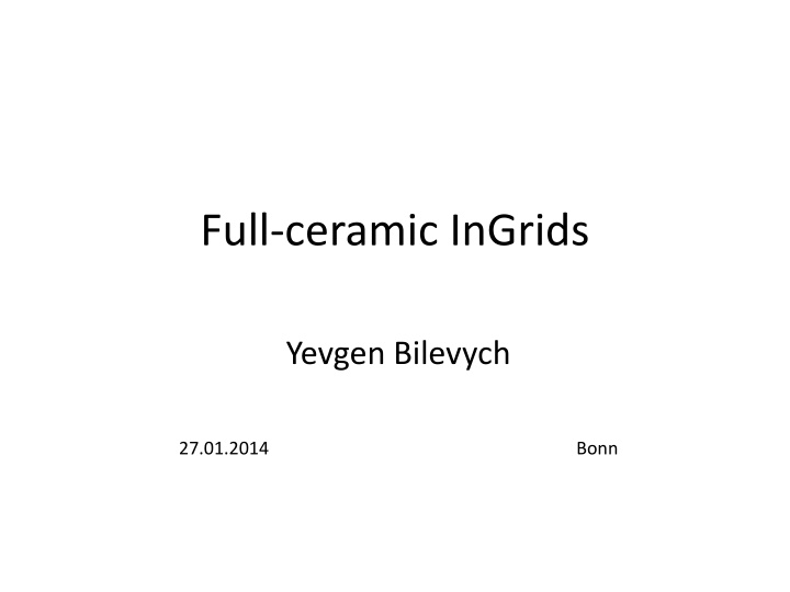
Full-ceramic InGrids Yevgen Bilevych 27.01.2014 Bonn
Ceramic grid Metal grid top view Grid cross-section
Ceramic grid short process-flow Dry etching of silicon Silicon oxide deposition Wafer bonding Wafer grinding Bottom Grid protection layer Metal electrode formation Top protection layer deposition Ceramic layers patterning Ceramic Grid releasing
1 m Si oxidized to 2,17 m 85-140 m 200-360 m 15-20 m 110 m
????? Alignment marks 2 times Dicing or cracking 2 layers of SixNy or only top-layer Thickness of SiO2 Thickness of metal layer Thermal stability of bonding material Possibility of bonding to chip or to wafer afterwards

")
")
")