Advanced CMOS Circuit Designs and Operational Amplifiers
Explore the world of CMOS circuits and operational amplifiers with detailed insights on differential amplifiers, mirror loads, output swings, and transconductance amplifiers. Learn about improving output swings, OTA analysis, and utilizing OTAs as transconductance amplifiers. Discover the significance of n-type and p-type OTAs working in collaboration for optimal performance in electronic systems.

Uploaded on | 0 Views
Download Presentation

Please find below an Image/Link to download the presentation.
The content on the website is provided AS IS for your information and personal use only. It may not be sold, licensed, or shared on other websites without obtaining consent from the author. If you encounter any issues during the download, it is possible that the publisher has removed the file from their server.
You are allowed to download the files provided on this website for personal or commercial use, subject to the condition that they are used lawfully. All files are the property of their respective owners.
The content on the website is provided AS IS for your information and personal use only. It may not be sold, licensed, or shared on other websites without obtaining consent from the author.
E N D
Presentation Transcript
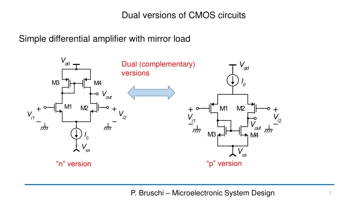
Dual versions of CMOS circuits Simple differential amplifier with mirror load Dual (complementary) versions p version n version P. Bruschi Microelectronic System Design 1
Ranges of the p version (0) = - V V V ( ( ( ) ( ) iC V ) ) = min = - + V V V DSAT V 3 out dd GS 2 2 out C GS V max = - V V 4 out dd DSAT min + + V V MIN tail V V V - 1 iC ss GS max = - - + V DSAT V V 3 1 1 dd GS GS ( ( ( ) C V ( ) V ) ) min = + V V DSAT V V 4 out ss max = + - V V DSAT V 2 + 2 out C GS min = + - V V DSAT V V 3 1 1 ss GS GS (0) = V V max = - - V MIN tail V V 3 out GS - 1 C dd GS P. Bruschi Microelectronic System Design 2
Ranges: graphical representation Input CM range Output swing n-type n-type p-type p-type P. Bruschi Microelectronic System Design 3
Improving the output swing: the OTA OTA: Operational Transconductance Amplifier The term OTA generally indicates all single-stage amplifiers with high output resistance. The folded cascode amplifier is often classified as an OTA. Historically, the term OTA has been used to indicate the topology shown in this slide P. Bruschi Microelectronic System Design 4
OTA: simple analysis = A G R d m out ( ) I k I I k g v @ - @- k : 1 1 : k 2 1 1 OCC D D m d kID2 = - G kg kID1 1 m m IOCC 1 + = / / = R r r 6 8 out d d l I l I kID1 6 6 8 8 D D = = I I kI 1 : 1 6 8 1 D D D 1 1 1 + I = - = A kV 1 D d ( ) ( ) + kI l l V l l 1 1 6 8 1 6 8 TE D TE P. Bruschi Microelectronic System Design 5
Usage of the OTA as a transconductance amplifier Gm-C Integrator iC OTA symbol 1 G sC ( ) = = - m V i V V 2 1 out c sC 1 1 P. Bruschi Microelectronic System Design 6
OTA output swing Output swing Input CM range P. Bruschi Microelectronic System Design 7
OTA with rail-to-rail input CM range Input CM range The idea is to make an n-type and p- type OTAs work together, In this way, for any value of the input common mode range, there is at least one OTA that operates correctly n-type p-type P. Bruschi Microelectronic System Design 8
OTA with rail-to-rail input CM range + ( ) ( ) - I I = - I I I 12 11 D D 22 21 OCC D D n P. Bruschi Microelectronic System Design 9
OTA rail-to-rail: equivalent Gm and dc gain ( ) ( + ) = - - I I I I I 22 21 12 11 OCC D D D D @ I G v OCC m d @ + I mp d g v mn d g v OCC = + G g g m n - m p - m n 1 + = / / = R r r 01 02 out d d l I l I 01 01 02 02 D D P. Bruschi Microelectronic System Design 10