Crystal Structure and Classification of Solids Based on Particle Arrangement
Solids are classified into crystalline and non-crystalline based on the arrangement of constituent particles. Crystalline solids exhibit a regular repetitive pattern in three dimensions, while non-crystalline solids lack such order. The structure of metals includes body-centered cubic (BCC), face-centered cubic (FCC), and hexagonal close-packed (HCP) arrangements. These structures determine the properties and behavior of materials.

Download Presentation

Please find below an Image/Link to download the presentation.
The content on the website is provided AS IS for your information and personal use only. It may not be sold, licensed, or shared on other websites without obtaining consent from the author. Download presentation by click this link. If you encounter any issues during the download, it is possible that the publisher has removed the file from their server.
E N D
Presentation Transcript
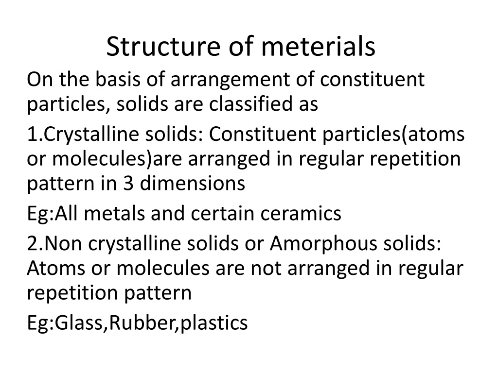
Structure of meterials On the basis of arrangement of constituent particles, solids are classified as 1.Crystalline solids: Constituent particles(atoms or molecules)are arranged in regular repetition pattern in 3 dimensions Eg:All metals and certain ceramics 2.Non crystalline solids or Amorphous solids: Atoms or molecules are not arranged in regular repetition pattern Eg:Glass,Rubber,plastics
Crystalline and Amorphous solids Amorphous Amorphous
Space lattice 3 dimensional network of imaginary lines connecting atoms in a crystal Intersection points are called lattice points which have identical surroundings Unit Cell The smallest portion of the space lattice which when repeated in all direction give rise to lattice structure It is the building block of crystal structure Bravais showed that there are 14 standard space lattices
Crystal structure of metals 1. Body centered cubic(BCC) One atom at each corners and one at the centre of cube At room temperature iron exhibit BCC structure Other metals possessing this structure are V,Mo,W,Cr,Ba etc Atomic packing factor 0.68 Coordination No: 8
2. Face centered cubic(FCC) Atoms are located at corners and at the centre of each cubic face More density packed than BCC Metals possessing this structure are Cu,Al,Pb,Ag etc Atomic packing factor 0.74 Coordination No: 12
Hexagonal close packed (HCP)structure One atom at each corner of hexagon One atom at centre of each hexagonal face (basal planes) 3 atoms in the form of a triangle midway between 2 basal planes Found in metals like Mg,Be,Ca,Zn,Cd & Ti Atomic packing factor 0.74 Coordination No: 12
Crystal growth and grain formation(Dendritic solidification) Crystallization is the formation of crystals(grains) during phase transformation of metals from liquid to solid state Occurs by nucleation and growth Nucleation: Atoms of liquid bond together and form nuclei(basic crystal structure) Growth :Nuclei grow in size with the addition of atoms Smallest unit of repetition is called unit cell Unit cells arrange themselves in straight lines forming primary arm. Secondary arm branches off from primary arm and tertiary arms from secondary arm producing dendritic structure Dendritic arms impinge each other at contact surface and forms grain boundaries Space between the arm solidifies to form grains
Grain size control Following factors controls the grain size Slow cooling results in large grains(coarse) where as fast cooling results in small grains(fine) Metallic and non metallic inclusions Mechanical working processes like rolling, forging etc Alloying elements Heat treatment process
Effect of grain size on properties of metals Fine grained materials possess improved strength, resistance to impact and cracking, better finish in deep drawing .They are preferred for structural application Coarse grained materials possess more ductility, malleability, machinability, hardenability and better creep strength .They are less tough and have greater tendency for distortion than fine grained materials. They are preferred for high temperature application
Grain size measurement The grain size specified by ASTM,American society for Testing and Materials is n = 2N-1 n= No. of grains per square inch at magnification of 100 X N= grain size No. Grain size no. 1 to 5 indicate coarse grained steel,6 to 10 indicates fine grained steel
Bonding in solids Types of bond I. Primary bond ionic, covalent and metallic II.Secondary bond (Molecular bond) Ionic bond : Exist between a metallic and non metallic atom.Eg:NaCl The Na atom gives away its valance electron to Cl atom producing Na + ions and Cl ions. Two oppositely charged ions attract and forms bonds
Covalent Bond Electrons are shared (not transferred ) between atoms Shared electrons are considered belonging to both atoms Eg:In molecule of methane(CH4) , carbon atom has 4 valence electrons where as each of the four hydrogen atom has single valence electron. So carbon and hydrogen share their electron to form covalent bond and become stable
Metallic bond Found in metals and their alloys Metallic atoms give up their valence electron and become positive charge ions The free electrons forms electron clouds and are surrounded by these positive ions Mutual force of attraction between positive ions and negative electron cloud forms metallic bond
Ionic bond Covalent bond Metallic bond Higher bond strength than metallic bond Higher bond strength than metallic bond Lower bond strength than other primary bonds Forms due to electrostatic force of attraction between +ve and ve ions of different elements Forms due to electrostatic force of attraction between atoms of same or different elements by sharing of electrons Forms due to electrostatic force of attraction between + ve ions and ve electron cloud of same or different metals Low electrical and thermal conductivity Low electrical and thermal conductivity High electrical and thermal conductivity High melting and boiling point Low melting and boiling point High melting and boiling point Exists in solids state only Exists in solids, liquids and gaseous form Exists in solids only(except Hg) Crystalline in nature Non crystalline Crystalline in nature High hardness Low hardness except diamond, silicon ,carbide Soft Soluble in water Not soluble in water. Soluble in organic solvents like benzene, toluene etc. Not soluble in water or organic solvents Not malleable and ductile Not malleable and ductile Malleable and ductile
Secondary bond Formed due to weak Van der Waals force of attraction between various atoms 3 types Dispersion bond Permanent dipole bond Hydrogen bond 1. Dispersion bond In a symmetrical molecule, centers of positive and negative charges coincide But if the centers of positive and negative charges do not coincide, the molecule will develop a small net fluctuating charge on each end The fluctuating charge on one molecule interact with fluctuating charge of neighboring molecule resulting in dispersion bond
1. Dispersion bond Fig1:Distribution of electronic charges in helium Fig2: Formation of dispersion bond in helium
2.Permanent dipole bond(Dipole-dipole bond) Due to unequal sharing of electrons between two atoms, opposite charges will be created and permanent dipole is produced Such dipoles attract each other and forms dipole- dipole bond E.g.: Even though hydrogen fluoride molecule is formed by covalent bond there is an electrical imbalance because the shared electrons are more close to nucleus of fluorine atom than nucleus of hydrogen atom This way an electrical dipole is created. Dipoles of opposite charges attract permanent dipole bond each other forming Covalent bond have equal sharing of electrons by two atoms
2.Permanent dipole bond(Dipole- dipole bond)
3.Hydrogen bond Special type of dipole bond Produced when hydrogen atom of one molecule is attracted to highly electro negative atoms(F,O,N) Eg:In H2O,the hydrogen electrons are more attracted towards oxygen atom (oxygen atom is more electro negative than hydrogen) inducing small +ve charge on hydrogen atom and small ve charge on oxygen atom and thus creating a dipole leading to bonding
Crystal defects(Crystal imperfection) In ideal crystal atoms are arranged in regular way In actual cases the arrangement of atoms are disrupted These disruption is known as crystal defects or imperfections
Classification of crystal defects 1. Point defect or zero dimensional defect They are imperfect point like region in a crystal Various point defects are a. Vacancy An atom missing from regular lattice position b. Self interstitial When an extra atom within the crystal occupies a space between regularly positioned atoms in a crystal
c.Substitutional and interstitial impurity Impurity is the presence of foreign atoms in a crystal Substitutional:When impurity atom occupies the void space where regular atoms are missing Interstitial :A small sized impurity atom occupying void space with out disturbing parent atom from their regular sites
Frenkal defect: Combination of vacancy and interstitial defect An ion displaced from normal lattice site to interstitial site Cations(+ ve ion) being smaller than anion(- ve charge) is displaced to void space Schottky defect: A pair of cations and anions missing from lattice site of an ionic crystal Closely related to vacancy *Frenkal and shottky defects are found in ionic crystals
2.Line defects or dislocations One dimensional defects Disturbed region between two perfect part of a crystal Responsible for slip by which metal deforms plastically Two types 1. Edge dislocation 2.Screw dislocation
Edge dislocation: An extra half plane of atoms either above or below the slip planes Magnitude and direction of dislocation is expressed in terms of Burgers vector The vector is at right angle to edge dislocation It is determined by drawing a rectangle in the region under consideration by connecting equal no. of atoms on opposite side and if certain region contains an edge dislocation, the circuit will break
2.Screw dislocation Shear stress applied on the crystal causes a portion of crystal to be shifted relative to other Arrangement of atoms appears like screw.so it is called screw dislocation Burgers vector is parallel to line dislocation
3.Surface defects 2 dimensional in nature 3 types 1. Grain boundaries The region that separates two adjacent grains of different orientation in a polycrystalline material At the grain boundaries atoms are not arranged perfectly and hence disturbed region is formed When orientation difference between neighbouring grains are more than 10 15 are called high angle grain boundaries Orientation difference is less than 10 are called low angle grain boundaries or tilt boundaries Tilt boundary is composed of edge dislocation lying one over the other
3.Twin boundary Produced due to mechanical shearing forces and annealing heat treatment The arrangement of atoms on one side of the boundary is mirror image of that of the other side
Miscellaneous defect-Stacking fault Formed when atoms are arranged in a sequence other than normal sequence Occurs in FCC when there is interruption in ABCABCABC stacking sequence Occurs in HCP when there is interruption in ABABAB stacking sequence
Volume defect These include pores, cracks, foreign inclusions etc. Introduced during processing and fabrication
Mechanism of plastic deformation in metals Plastic deformation of metals occurs by slip and twinning 1.Slip Permanent deformation of one part of crystal relative to the other. Slip involves sliding of one plane of atoms over the other under the influence of shear force. 2.Twinning Atoms of a part of crystal when subjected to stress are displaced so that the twinned portion of the crystal is a mirror image of the parent crystal
SLIP AND TWINNING Twinning Slip process
Property changes by deformation- work hardening, solid solution hardening, and precipitation hardening 1. Work hardening or Strain hardening Process of making metal stronger through plastic deformation by cold working Used for metals which are least responsive to heat treatment Plastic deformation is caused by dislocation movement When material is cold worked, there will be an increase in dislocations which will interact with other moving dislocations The interacting dislocations lead to decrease in their mobility (*similar to traffic jam) and hence material get strengthened Work hardening reduces ductility and plasticity


")

structure")
structure")


")


")