Innovations and Transformations in Condensed Matter Physics
Accelerating mainstream developments in condensed matter physics involves inducing electronic states and phases through strong external influences like electric or optical impacts. Notable successes include superconductivity manipulation and laser-induced transformations, with significant contributions from institutions like Bell Labs and researchers like John Bardeen. The pursuit of alchemical transformations in material properties through Electrostatic Doping remains a compelling research area in modern physics.

Download Presentation

Please find below an Image/Link to download the presentation.
The content on the website is provided AS IS for your information and personal use only. It may not be sold, licensed, or shared on other websites without obtaining consent from the author. Download presentation by click this link. If you encounter any issues during the download, it is possible that the publisher has removed the file from their server.
E N D
Presentation Transcript
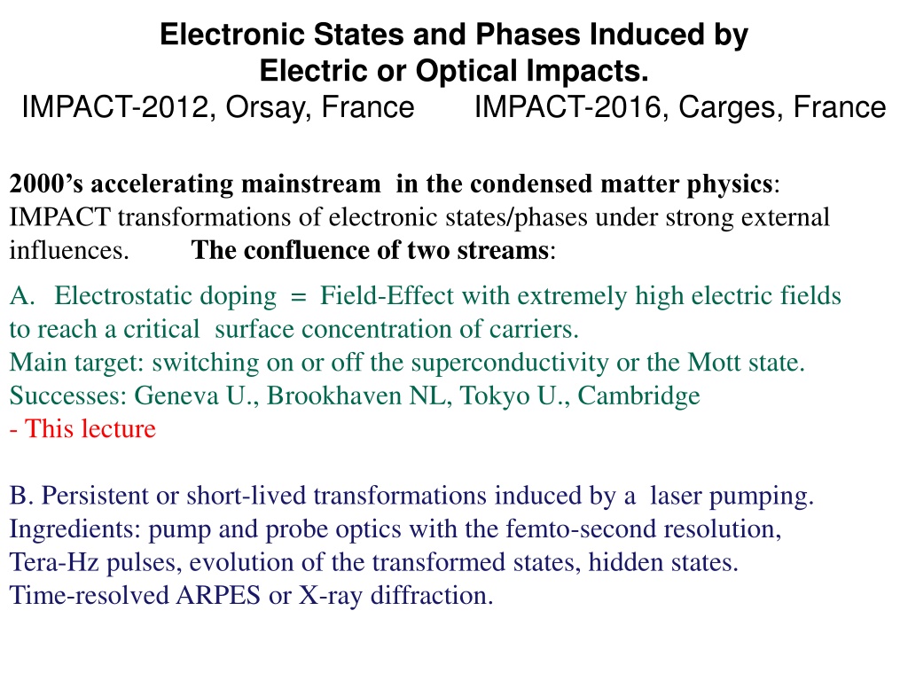
Electronic States and Phases Induced by Electric or Optical Impacts. IMPACT-2012, Orsay, France IMPACT-2016, Carges, France 2000 s accelerating mainstream in the condensed matter physics: IMPACT transformations of electronic states/phases under strong external influences. The confluence of two streams: A. Electrostatic doping = Field-Effect with extremely high electric fields to reach a critical surface concentration of carriers. Main target: switching on or off the superconductivity or the Mott state. Successes: Geneva U., Brookhaven NL, Tokyo U., Cambridge - This lecture B. Persistent or short-lived transformations induced by a laser pumping. Ingredients: pump and probe optics with the femto-second resolution, Tera-Hz pulses, evolution of the transformed states, hidden states. Time-resolved ARPES or X-ray diffraction.
Unrivaled glory of Bell Labs, from the mighty ATT Transistors, field-effect transistor (MOSFET); Zone melting for semiconductors; Molecular beam epitaxy; CCD: charge-coupled device (digital cameras, Hubble); Lasers (gas, semiconducting, organic), quantum cascade IR laser; Laser cooling of atoms; Fractional quantum Hall effect; Radio astronomy, background radiation from the Big Bang; Information theory, codes for error detection and correction. Unix operating system, C, C++ programming languages; Shor quantum factorization algorithm, Digital cellular telephone technology, Fiber optic Theoretical physics (PW Anderson at the top) 8 Nobel Prizes
John Bardeen Nobel Prizes in Physics 1956 and 1972 The personal synergy of inventions in semi- and superconductivity; now it is materialized through experimental achievements of 2000 . Bardeen, Shockley and Brattain 3
Bell Labs within Lucent Technologies: struggling the decline. Jan Hendrik Sch n affair 2000-2003 Claims for possessing an alchemical gold : the philosopher stone transforming any material to any electronic state by means of the Field-Effect = Electrostatic Doping Publications in Science alone: "Ambipolar Pentacene Field-Effect Transistors and Inverters "A Superconducting Field-Effect Switch". "Fractional Quantum Hall Effect in Organic Semiconductors "An Organic Solid State Injection Laser". "A Light-Emitting Field-Effect Transistor". "Josephson Junctions with Tunable Weak Links "High-Temperature Superconductivity in Lattice-Expanded C60". "Field-Effect Modulation of the Conductance of Single Molecules". Science withdrew these eight papers written by Sch n with senior coauthors + as many from other top journals
The earlier injection transistor was used for signal amplification (the Sony walkman proclaimed the mineaturization epoch) The modern choice for switching is the FET field effect transistor Gate voltage controls the concentration of carriers between the source S and the drain D electrodes The operation scale: 10-6 e/site. Dream: get 10-1 e/site to reach transitions to new electronic states Price: need almost intra-atomic scales of the electric field.
Field effect dream to transform any material to any electronic state. Anticipating a tunable superconductivity Bell Labs, H.Shoen affair its very negative and well stimulating impact 2002 Darkness in the Murray Hills tunnel 2002 + Side light at the Alpine tunnel section - Geneva. 2003 + Light at the Pacific end of the tunnel - Japan. 2010 Explosions of studies on oxides and organic conductors. 1980/90 s Theorists calling Russia, Swiss. Goal: create a field effect injection up to ~10% per surface unit cell. Ingredients of modern research: Active material, accepting either electrons or holes, and possessing different , tunable insulating , metallic, superconducting ground states : High-Tc superconductors - cuprates and pnictides - in antiferromagnetic states, transition metals oxides with charge- and orbital- ordering and magnetism, transition metals halcogenides with charge density waves, organic conductors with the charge ordering, conducting polymers.
Field effect transistor, FET. Metal oxide semiconductor FET (MOSFET) Gate Source Gate dielectric Drain Active material Field effect transistor, FET x~10-6el/atom High-temperature superconductors - - - - - - - Need x~0.1 el/atom ! Requires for the electric field E>10MV/cm
Untimely theories 1. Early 80 s, rise of conducting polymers. Metallization of polyacetylene by doping 1979. Dissatisfaction about effects of charged disorder. Additional intrigue: Firm theoretical and experimental grounds for formation of bipolarons 2-electron particles, prone to superconductivity. Desire: to obtain them in a pristine state. Hence two suggestions: a. S. B. and N. Kirova 1981 Call for optical pumping of solitons b. S.B. N.K. and V. Yakovenko , Solid State Commun. 1985 "On the possible superfluidity of bipolarons at the junction surface
2. Late 80s, Epoch of high-Tc superconductivity. Dissatisfaction about effects of charged, substitutional and oxygen disorders. Intrigue: Intrinsic relation of the superconductivity in the doped state and the pristine antiferromagnetic Mott insulator Desire: to obtain the superconductivity without doping. Hence the suggestion: Possible superconductivity on the junction surface of dielectric La2CuO4 S. B. and V. Yakovenko, ... induce excess charge on the surface of the dielectric La2CuO4 by the field effect transistor or in the Schottky junction. ... Superconductivity can be observed in this two dimentional system to manufacture superconducting devices controlled by electric field JETP Let. & Phys. Let. 1988 J. Mannhart and A. Baratoff, "Superconducting p-n junctions" 1993 Possibility to explore existence of both n- and p- doped cuprates.
Feasibility of the extreme Field Effect as seen 2 decades ago V. Yakovenko 1988, unpublished. Achievable concentrations of electrons at the surface of the CuO2 plane for different gate dielectrics. x=15% was most wanted. D ED 107V/cm 2.4 - 6 Dielectrics ED 106V/cm 6 D n= DED/4 e 1013 cm-2 1.3 3.3 x=n(3.8A)2 in % - 10-2 1.9 4.8 SiO2 4- 10 Al2O3 5 8 - 9 4 4.5 2.2 - 2.5 3.2 3.6 2.5 3.6 Y2O3 5 9 - 13 4.5 6.5 3.6 5.2 HfO2 50 15 75 41.4 60 PbTiO3 0.5 30 - 200 1.5 10 0.83 5.5 1.2 7.9 Notice the promising case of HfO2 gate. Exotic in mid-80's, it became a working material today, in epoch of high-K and 20 s nm. 10
Experimental Strategy Pure FET Achievements Insulator - Metal transition in SrTiO3 2003 AIST, Tsukuba Miyano 2005 (Tokyo U.) Pure optical pumping, no gate. R1-xAxMnO3 Transformation : charge-orbital ordered insulator --> ferromagnetic metal Triscone 1999 Geneva) Bozovic (BNL, USA) Reyren 2007, Triscone 2008 MBE+ ferroelectric Electrostatic Modulation of Superconductivity in GdBa2Cu3O7 x MBE Molecular Beam Epitaxy Variable atomic layeres SC at interface of LaAlO/SrTiO3 Photoinduced IMT VO2, TiO2, LaSrMnO3 CaCuO2 Surface carrier density reached 1015 /cm2 Superconductor insulator transition in La2-xSrxCuO4 Hiroi 2002 (ISSP, Japan) Gate voltage + optical pumping across the gate Double-Layer Transistor by electrolyte gating Iwasa 2008 (Tokyo ) Bozovic 2011 (BNL, USA)
Direct assault at a minimal possible frontier. Micro gate area may have no leakage defects. Field effect doping of SrTiO3 Inoue et al, CERC AIST, Tsukuba, Japan Drain current ID (solid line) and the charge mobility (dashed line) plotted against the gate electric field EG 10K 12
Strategy 2. Direct assault, pure optical pumping, no gate. Photoinduced insulator-to-metal transition K. Miyano & N. Takubo, University of Tokyo. 2005 Perovskite manganites, R1-xAxMnO3 (compounds of the colossal magnetoresistance) Transformation : charge- and orbital-ordered insulating (COOI) state ferromagnetic metallic (FMM) phase Laser pulse (a) 8 10 Pr0.55(Ca1-ySy)0.45MnO3 film on (LaAlO3)0.3(SrAl0.5TaO3)0.7 (110) substrate, y = 0.25 Photon energy is 2.3 eV Laser pulses transform COOI FMM 7 10 Resistance ( ) 6 10 5 10 4 10 3 10 100 150 200 250 Temperature (K)
Strategy 3. Combination of the gate voltage with the optical pumping across the gate Photocarrier Injection to Transition Metal Oxides Y. Muraoka and Z. Hiroi -- ISSP, Japan Estimated photo-doping: ~1020/cm3 , i.e. 1% per atom
4. Gigantic amplification of the gate voltage in the field effect by adding the ferroelectric layer. Electrostatic Tuning of the Hole Density in NdBa2Cu3O7-x Films and its Effect on the Hall Response J.-M. Triscone group, Geneve. Phys. Rev. Let. 2002 (first results 1999) Ferroelectric gate switching requires only a voltage pulse, Persistent reversible effect. Achieved: switching off of the superconductivity in a pre-doped material. Still necessary: turn the SC on from the pristine undoped insulator 15
Local switching of two-dimensional superconductivity using the ferroelectric field effect J.-M. Triscone, et al Nature 441 (2006) 195 The P+ state - removing electrons from the Nb-STO layer. The P- state - adding electrons to the Nb-STO layer (increasing the doping)
Today: nanoscale manipulations (Villegas et al, Thales, France) Magnetic flux vortices BiFeO3 (BFO) P 100 C/cm2 YBa2Cu3O7- (YBCO) Tc=92 K 17
Iterdisciplinary: gate dielectric - electrolytic condensor from polymeric FET (Invented for doping by/of conducting polymers)
Polymer Electrolyte-Gated Organic Field-Effect Transistors M. J. Panzer and C. D. Frisbie Still, the J. of American Chemical Society Univ. of Minnesota mid-2000 s Physics journals at last: PNAS2006, + |NMAT 2009
Electric-field-induced superconductivity in an insulator Iwasa group (Sendai) Nature Materials 7 (2008) 855; 9, 125 (2010). R.H. Friend group (Cambridge UK): Adv. Mater. 22, 2529 (2010). pristine SrTiO3 as chanel, liquid solid electrolyte as gate dielectric Cations (K+) in the electrolyte are solvated by polyethylene oxide molecules and are electrostatically adsorbed on the SrTiO3 VG = 3.5 V, n2D > 1014 cm 2, cf. FIT record n2D ~ 1 1013cm 2 25
Strategy 6: hybrid of 4 and 5 - Electrolyte upon the MBE MBE molecular beam epitaxy LaTiO3 layers (bright lines) of varying thickness separated by varying thicknesses layers of SrTiO3 (darker regions). Upper panel: magnified view of the 51 region
Superconductorinsulator transition in La2-xSrxCuO4at the pair quantum resistance, Nature, 472 (2011) 458 I.Bozovic group synthesis of epitaxial films of La2-xSrxCuO4 (x=0.06 0.20) 1, 1.5, 2 unit cell thick, and fabrication of double-layer transistors(NaF+polyethylene glicole) Optimal doping 0.15 At low concentration SC disappears via Bose glass phase without pair breaking Achieved: switching off of the superconductivity in a pre-doped material. Still necessary: turn the SC on from the pristine undoped insulator
The goals are to deplete carriers and to traverse the transition to the insulator, to add carriers to cross over the top of the dome and to deplete carriers for the crossover from the insulator to the electron doped regime.
IMPACT-2012 30
Further depletion of holes 1.52V 0 120k 1.52 V 12k 1.2k Rs( ) 0 V 120 12 1.2 0 20 40 60 80 100 120 140 T(K)
Recall J. Mannhart and A. Baratoff, "Superconducting p-n junctions" 1993 Possibility to explore existence of both n- and p- doped cuprates.
Additional, or even the main, reason for attention: Two-photon channel of cooper pairs recombination And these photons are entangled!
Auxiliary Material: A bit of the old theory
Polymers Doped Undoped FET MOSFET junction allows to introduce charge, hence to create bipolarons on the junction surface Advantages: no additional disorder Problems: Wigner crystallization dipole formation High electric field Bipolarons: volume concentration depends on the doping level But: dopant induced disorder supresses the possibility Bose condensation also in homogeneous material A chance for Bose condensation
Superconductivity from the Bose-condensation of bipolarons or of prefabricated Cooper pairs at the junction surface: after S.B. N.K. and V. Yakovenko , Solid State Commun. 1985 Some theory problems to be solved: In conventional Bose condensation the number of particle is fixed. In FET the electrochemical potential is monitored by external electric field no ideal BEC. 2D ideal gas: Condensation is not allowed in any sense 2D non ideal gas: Bose condensation is possible in a sense of Beresinski-Kosterlitz-Touless Specific questions: effects of Coulomb forces values of the required electric field
2 2 ( 2 ) d z + ) = ( ( ) 0 0 V z z Model 0 2 M dz d 2 ( 2 ) V z + 2 = 2 0 4 ( ) 0 e z 4 dz 0(z/z0) 0.5 Formation of the self-consistent potential wall with the single localized eigenstate at the given eigenvalue of . Screening by the single wave function. 0 (z/z0) 10 V(z/z0) Electric field E~107eV -1 40
Conclusions and perspectives Field effect electrostatic switching of electronic states at the surface is well confirmed by diverse experimental methods The 2D, even monolayer superconductivity does exist Methodic progress raised the scale of manipulation from mK to 30K Non realized or unattended issues: Ambipolar switching Realization of semi super devices. Superconducting p-n junction 41