Programmable Interface Devices 8155/8156 Overview and Design Considerations


Asst. Lec. Lubna A. Alnabi

Third Class
Real Time System Design
Programmable Interface Devices
8155/8156


Programmable Interface Devices
8155/8156

Programmable Interface Devices

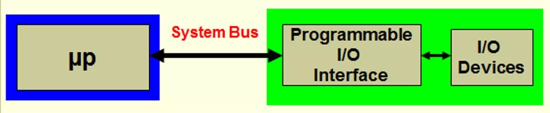
•
Used to interface an I
/
O device to the
microprocessor.
•
Can be programmed
/
configured to
perform various I/O functions by writing
software instructions.
Programmable Interface Devices
8155/8156
8155/8156 – A Multipurpose Programmable Interface
Its programmable interface device used to interface I/O
device to μP, its multifunction device, contain RAM, I/O
ports, and timer.
•
Designed to be compatible with 8085.
•
It includes:
• 256 bytes of Read/Write memory.
• Three I/O ports (programmable I/O):
o Port A (8-bit).
o Port B (8-bit).
o Port C (6-bit).
• A 14-bit timer.
Programmable Interface Devices
8155/8156
Programmable Interface Devices
8155/8156
8155 block diagram shows 5 control signals, all except (CE)
are input signal directly generated by the processor; the
(CE) is input from decoder.
o CE: chip enable, connected to the decoder.
o IO/M: specify whether the memory section is selected, or
I/O section (include timer) is selected.
o ALE: address latch enable.
o RD and WR
o RESET: connect to the RESET out of processor used to
reset the chip and initializes I/O ports as input.
• In 8155 we have control register, 3 I/O ports, and 2
register for timer, so we need 3 address lines to decode
there register.
Ex:
design (draw) and determine the address of the
control/status, I/O ports and timer register of the 8155
if the output of decoder O2?
Control word (command reg) format
Ex:
Design an interfacing circuit to read data
from an A/D converter using the 8155A in the
peripheral mapped I/O.
Explore the capabilities of programmable interface devices 8155/8156 for interfacing I/O devices to microprocessors. Learn about their features, block diagrams, control signals, and address determination. Discover how to design interfacing circuits for reading data from A/D converters using the 8155A in peripheral mapped I/O settings.

Download Presentation

Please find below an Image/Link to download the presentation.
The content on the website is provided AS IS for your information and personal use only. It may not be sold, licensed, or shared on other websites without obtaining consent from the author. Download presentation by click this link. If you encounter any issues during the download, it is possible that the publisher has removed the file from their server.
E N D
Presentation Transcript
Third Class Real Time System Design Programmable Interface Devices 8155/8156 Asst. Lec. Lubna A. Alnabi
Programmable Interface Devices 8155/8156 Programmable Interface Devices Used to interface an I/O device to the microprocessor. Can be programmed/configured to perform various I/O functions by writing software instructions.
Programmable Interface Devices 8155/8156 8155/8156 A Multipurpose Programmable Interface Its programmable interface device used to interface I/O device to P, its multifunction device, contain RAM, I/O ports, and timer. Designed to be compatible with 8085. It includes: 256 bytes of Read/Write memory. Three I/O ports (programmable I/O): o Port A (8-bit). o Port B (8-bit). o Port C (6-bit). A 14-bit timer.
Programmable Interface Devices 8155/8156
Programmable Interface Devices 8155/8156 8155 block diagram shows 5 control signals, all except (CE) are input signal directly generated by the processor; the (CE) is input from decoder. o CE: chip enable, connected to the decoder. o IO/M: specify whether the memory section is selected, or I/O section (include timer) is selected. o ALE: address latch enable. o RD and WR o RESET: connect to the RESET out of processor used to reset the chip and initializes I/O ports as input. In 8155 we have control register, 3 I/O ports, and 2 register for timer, so we need 3 address lines to decode there register.
Ex: design (draw) and determine the address of the control/status, I/O ports and timer register of the 8155 if the output of decoder O2?
Ex: Design an interfacing circuit to read data from an A/D converter using the 8155A in the peripheral mapped I/O.


 and determine the address of the")
 format")
 format")