VHDL Signal Generator, PWM Generator, and Pattern Generator Systems
Explore VHDL programs for signal generators, PWM generators, and pattern generator systems with various specifications like clock inputs, reset signals, and output patterns. Dive into entity declarations and architecture bodies for different systems, including synchronous and asynchronous resets. Design a state machine with states s0, s1, s2, and s3 that changes based on clock signals and input conditions, providing corresponding output states.

Download Presentation

Please find below an Image/Link to download the presentation.
The content on the website is provided AS IS for your information and personal use only. It may not be sold, licensed, or shared on other websites without obtaining consent from the author. If you encounter any issues during the download, it is possible that the publisher has removed the file from their server.
You are allowed to download the files provided on this website for personal or commercial use, subject to the condition that they are used lawfully. All files are the property of their respective owners.
The content on the website is provided AS IS for your information and personal use only. It may not be sold, licensed, or shared on other websites without obtaining consent from the author.
E N D
Presentation Transcript
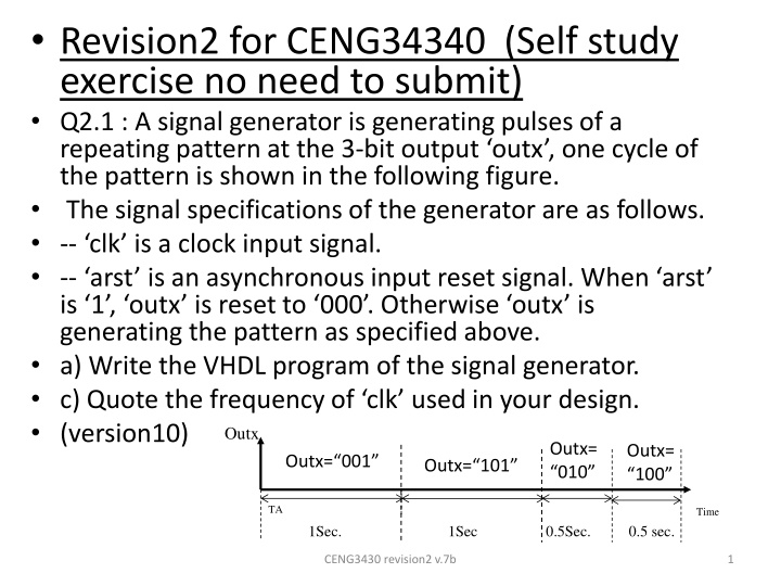
Revision2 for CENG34340 (Self study exercise no need to submit) Q2.1 : A signal generator is generating pulses of a repeating pattern at the 3-bit output outx , one cycle of the pattern is shown in the following figure. The signal specifications of the generator are as follows. -- clk is a clock input signal. -- arst is an asynchronous input reset signal. When arst is 1 , outx is reset to 000 . Otherwise outx is generating the pattern as specified above. a) Write the VHDL program of the signal generator. c) Quote the frequency of clk used in your design. (version10) Outx Outx= 001 Outx= 010 Outx= 100 Outx= 101 TA Time 1Sec. 1Sec 0.5Sec. 0.5 sec. CENG3430 revision2 v.7b 1
Q2.2 : These are questions on counters and pattern generators. A pulse-width-modulation (PWM) generator converts an 8-bit digital input Din into PWM pulses at the single bit output outy . One cycle of the PWM signal is 20ms and is shown below. The pulse on_time (y) is linearly proportional to the value of Din . Such that, when Din is 0 , y is 0, and when Din is 255, y is [255*(20/256)] ms, the signal specifications are as follows. clk is a clock input signal. Din is an 8-bit digital input signal. outy is an output signal for the PWM pulses. srst is a synchronous input reset signal. When srst is 1, outy is reset to 0. Otherwise outy is generating pulses as specified. Sketch 1 cycle of the waveform of outy when Din= 1 . Mark on your diagram the time (in ms) when outy changes states. Sketch 1 cycle of the waveform of outy when Din = 255 . Mark on your diagram the time (in ms) when outy changes states. Write the VHDL program of this signal generator. Quote the frequency of clk used in your design. (version10) Digital level High = 1 Low = 0 CENG3430 revision2 v.7b Time (ms) On_time =y Off_time=20ms -y 20ms : One cycle of the PWM pulses of outy 2
Q2.3 A pattern generator system has a reset input RST, an input TAG, a clock input C1 and an output X which is a vector consisting of X(2), X(1), X(0). Write the entity declaration of a VHDL program for the above interface signals. Write the architecture body in each of the following different systems. (System 1) The reset (RST) of the system is synchronous. The system is an up/down counter. After reset (RST=1), output X is cleared. When RST=0, the pattern generator is a binary up/down counter, at each rising edge of C1, output X changes states. When TAG=1, the continuous counting sequence at X is counting upward. When TAG=0, the continuous counting sequence at X is counting downward. (System 2) The reset (RST) of the system is asynchronous. Every time after reset (RST=1), output X is cleared. When RST =0, at each rising edge of C1, output X changes states depending on TAG as follows. (During counting, TAG and RST remain unchanged.) If TAG is 1, the counting sequence at X is 111 , 101 , 010 , 011 and then X remains unchanged until the next reset arrives (when RST=1). If TAG is 0, the counting sequence at X is 000 , 111 , 001 and then X remains unchanged until the next reset arrives (when RST=1). (Version 9) CENG3430 revision2 v.7b 3
Q2.4 :A state machine (having states: s0,s1,s2,s3) changes states at the rising edge of a clock (CLK). The input and output signals used are shown as follows. Clock input: CLK Asynchronous Input: RST, Synchronous Input: INX, Output: OUTX (3 downto 0) You are required to design the basic version of the state machine. When RST is 1 , the state is reset to s0, otherwise at each rising edge of CLK the state changes according to this pattern: s0 s1 s2 s3 back to s0 and so on. The output specification for each state is as follows. When INX is 1 , OUTX at state s0, s1, s2 and s3 are 1, 3, 5 and 7 (in hex) respectively. When INX is 0 , OUTX at state s0, s1, s2 and s3 are A,B,C and D (in hex) respectively. Hint: In VHDL you may write the value A in Hex as 1010 or x A . Write the VHDL entity declaration and architecture for the state machine. -You are required to modify the above version of the state machine based the following specification. Add a signal: OUTY (3 downto 0), which has a value representing the difference between the OUTX of the current state and OUTX of the previous state. Describe how to modify the state machine in part (a) to fulfil the requirement. You may rewrite the VHDL entity declaration and architecture, or show the instructions needed to be added. Hint: You may add additional signals to the system. (version 9) CENG3430 revision2 v.7b 4