Understanding Processor Technology and Memory Hierarchy Advancements
Explore advanced processor technologies including superscalar and vector processors, memory hierarchy concepts, virtual memory implementation, shared memory organizations, bus systems, and pipeline design. Delve into the design space of processors, comparing CISC and RISC architectures, and discover the evolution of multi-core, embedded, low-cost, and low-power processors.

Download Presentation

Please find below an Image/Link to download the presentation.
The content on the website is provided AS IS for your information and personal use only. It may not be sold, licensed, or shared on other websites without obtaining consent from the author. Download presentation by click this link. If you encounter any issues during the download, it is possible that the publisher has removed the file from their server.
E N D
Presentation Transcript
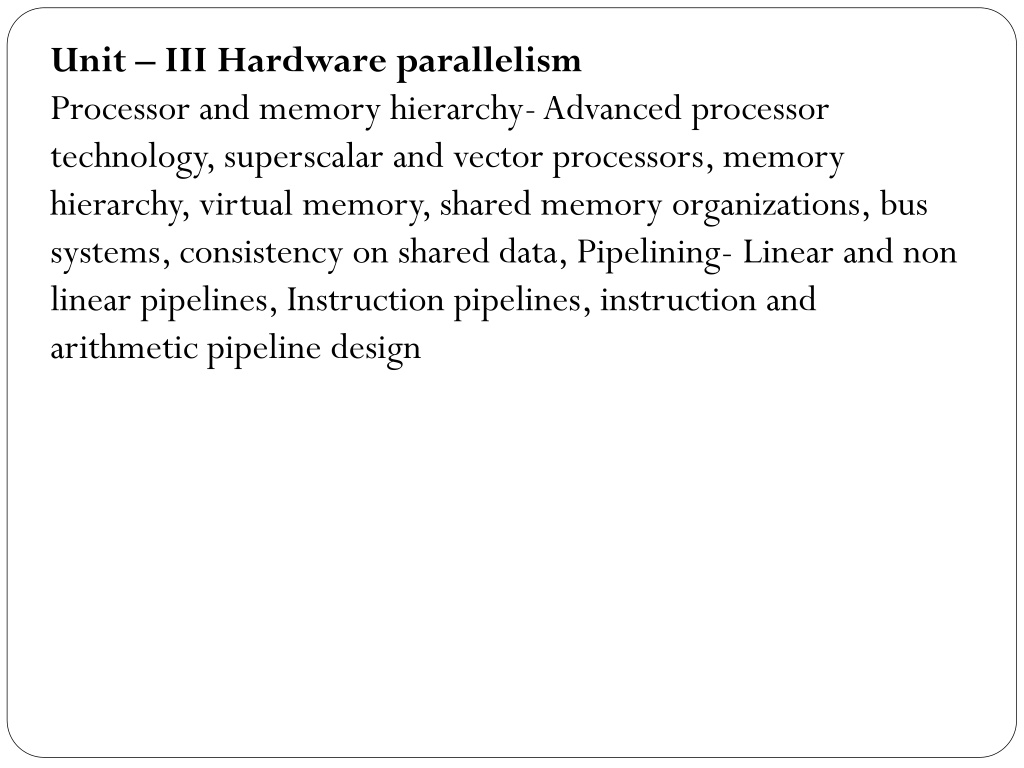
Unit III Hardware parallelism Processor and memory hierarchy- Advanced processor technology, superscalar and vector processors, memory hierarchy, virtual memory, shared memory organizations, bus systems, consistency on shared data, Pipelining- Linear and non linear pipelines, Instruction pipelines, instruction and arithmetic pipeline design
Processors and Memory Hierarchy Processors and Memory Hierarchy Advanced Processor Technology Today, large variety of technologically advanced multiprocessors exist. We need to understand their architectural advancements, Superscalar and Vector Processors architecture, their memory organization is also need to understand. Virtual memory concepts and issues involved in implementing it specially in multiprocessors also need to address.
Processors and Memory Hierarchy Processors and Memory Hierarchy Advanced Processor Technology .contd. 1. Design Space of Processors We can map the clock rate and cycles per instruction of advanced processors in the design space. New technology enables high clock rate. Therefore various processors are gradually moving from low to higher speeds towards right of the design space. Manufacturers trying to lower the number of cycles per instruction.
Multi-core, embedded, Low cost, low power High Performance 5 4 CISC 3 CPI 2 RISC 1 VP 1 2 3 Clock Speed (GHz)
CISC Processors: Examples of Complex Instruction Set Computing (CISC) processors are Motorola 68040, the VAX/8600, IBM S/390 and Intel 80486. CISC architecture uses microprogrammed control units which are having lower clock rates, and higher CPI and are located at the upper left of design space.
RISC Processors: Examples of Reduced Instruction Set Computing (RISC) processors are SPARC, MIPS R3000, IBM RS/6000 and Intel i860. RISC architecture uses hard-wired control units which are having higher clock rates, and lower CPI approximately one to two cycles and are located below CISC processors in design space.
RISC Scalar Processors: A special subclass of RSIC processors are the superscalar processors which allow multiple instruction to be issued simultaneously during the cycle. The effective CPI of a superscalar processor should be less than that of a generic scalar RISC processor. Clock rates of scalar RISC and superscalar RISC machines are similar.
Superpipelined Processors: These processors typically use a multiphase clock running at a relatively high rate. Actually several clocks, that are out of phase with each other, each phase controlling the issue of another instruction. Processors in vector supercomputers are mostly superpipelined and use multiple functional units for concurrent scalar and vector operations. They resides on lower right corner of the design space.
VLIW Architecture: Very Long Instruction Word machines typically have many more functional units. These machines uses microprogrammed control units with relatively slow clock rates because of the need to use ROM to hold the microcode. They resides on lower right corner of the design space.
Instruction pipeline The execution cycle of a typical instruction includes four phases: fetch, decode, execute and write back. These instructions are executed as instruction pipeline. Instruction pipeline cycle the time required for each phase to complete its operation (assuming equal delay in all phases)
Instruction issue latency the time (in cycles) required between the issuing of two adjacent instructions Instruction issue rate the number of instructions issued per cycle (the degree of a superscalar) Simple operation latency the delay (after the previous instruction) associated with the completion of a simple operation (e.g. integer add) as compared with that of a complex operation (e.g. divide). Resource conflicts when two or more instructions demand use of the same functional unit(s) at the same time.
A base scalar processor is defined as a machine with one instruction issued per cycle, a one-cycle latency for a simple operation, and one cycle latency between instruction issues. Instruction pipeline can be fully utilized if successive instructions can enter it continuously at the rate of one per cycle (figure a). IFetch Decode Execute Write-back Successive Instructions 0 1 2 3 4 5 6 7 8 9 10 Time in Base Cycles a) Execution in Base Scalar Processor
Instruction issue latency can be more than one cycle for various reasons. For example, if the instruction issue latency is two cycles per instruction, the pipeline can be underutilized (figure b) IFetch Decode Execute Write-back Successive Instructions 0 1 2 3 4 5 6 7 8 9 10 11 12 13 Time in Base Cycles b) Underpipelined with two cycles per instruction issue
Pipeline cycle is doubled by combining pipeline stages: Fetch and decode phases are combined into one pipeline stage, and execute and write-back are combined into another stage. This is also an example of poor pipeline utilization. Ifetch & Execute & Decode Write-back Successive Instructions 0 1 2 3 4 5 6 7 8 9 10 Time in Base Cycles c) Underpipelined with twice the base cycle
The effective CPI is 1 for the ideal pipeline (figure a), and 2 for other cases (figure b and c). According to the equation: I f I f = = = c c MIPS 6 6 6 10 10 10 T CPI C The cases in figure b and c will reduce the performance by one-half as compared with that of in ideal case.
Instruction Set Architectures Instruction set of a computer specifies the primitive commands or primitive instructions that a programmer can use in programming the machine. Complexity of an instruction set is depends on Instruction formats Data formats Addressing modes General purpose registers Opcode specifications, and Flow control mechanism used.
Two instruction set architectures are CISC and RISC Complex Instruction Set Computers (CISC) Based on microprogrammed control, evolved in 1960s and 1970s, many HLL functions are implemented directly in hardware/firmware. Typical CISC instruction set contains 120 to 350 instructions, 8-24 GPRs, execute large number of memory reference operations based on more than dozen addressing modes. Adv: Simplifies compiler development, improve execution efficiency, allow extension from scalar instructions to vector and symbolic instructions.
Reduced Instruction Set Computers (RISC) Based on Hardwired control. Evolved around 1990s, computer scientists found that only 25% of instructions of a complex instruction set are frequently used. It indicates that, about 75% of hardware supported instructions are rarely or not used at all. Designers vacate those 75% hardware supported instructions from firmware. This vacant chip area used to build more powerful RISC or superscalar processor. RISC instruction set contains less than 100 instructions, fixed instruction formats, three to five addressing modes, most instruction executes in one cycle, high clock rate, low CPI.
CISC and RISC architecture diagram Control Unit Instruction and Data path Hardwired Control Unit Data path Microprogrammed control memory Instruction Cache Data Cache Cache (Instruction) (Data) Main Memory Main Memory CISC architecture with microprogrammed control and unified cache RISC architecture with hardwired control and split instruction cache and data cache
Main features of typical CISC and RISC Architecture Architectural Characteristic Instruction set size and instruction format Addressing modes CISC RISC Large set of instructions with variable formats (16- 64 bits per instruction) 12 to 24 Small set of instructions with fixed format (32 bit) and most register-based instructions Limited to 3 to 5 GPRs and Cache design 8 to 24 GPRs Large number of GPRs (32 to 192) mostly with split data cache and instruction cache One cycle for almost all instructions, avg CPI < 1.5 Hardwired without control memory CPI CPI between 2 and 15 CPU Control Microcoded using control memory (ROM)
CISC Scalar Processors A scalar processor executes scalar data like integer instructions using fixed- point operands. Advanced scalar processors executes both integer and floating-point operations. CISC scalar processors can be pipelined based on complex instruction set. However, most of the times, CISC scalar processors are underpipelined (fig b and c) due to data dependence among instructions, resource conflict, branch penalties, and bad programming logic.
Digital Equipment VAX 8600 CPU, a typical CISC processor architecture VAX 8600 CPU contains two functional units for concurrent execution of integer and floating point instructions. Cache was used to hold both instruction and data. There are 16 GPRs in instruction unit with six stages of instruction pipeline. The Translation Lookaside Buffer (TLB) was used in memory control unit for fast generation of physical address from virtual address. Both integer and floating point units were pipelined. The processor performance is heavily depends on cache hit ratio. The system was later upgraded to VAX 9000 series providing vector hardware and multiprocessor options.
Representative CISC Scalar Processors of year 1990 Feature Intel i486 Motorola MC68040 NS 32532 (for PC) Instruction set size and word length 157 instructions 32 bit 113 instructions 32 bit 63 instructions 32 bit Addressing modes 12 18 9 Integer unit and GPRs 32-bit ALU with 8 registers 32-bit ALU with 16 registers 32-bit ALU with 8 registers On chip cache and memory management units (MMUs) 8-KB unified cache for both code and data with separate MMUs 4-KB code cache, 4-KB data cache 512-B code cache, 1-KB data cache Floating point unit registers and functional units On-chip with 8 FP registers, adder, multiplier, shifter On-chip with 3 pipeline stages, 8 80-bit FP registers Off-chip FPU NS 32381, or WTL 3164 Pipeline stages 5 6 4 Protection levels 4 2 2 Memory organization and TLB/ATC entries Segmented paging with 4KB/page and 32 entries in TLB Paging with 4 or 8 KB/page, 64 entries in each ATC Paging with 4KB/page, 64 entries 0.8 m HCMOS, 1.2 M transistors, 20 MHz, 40 MHz, 179 pins, 1990 1.25 m CMOS, 370K transistors, 30 MHz, 175 pins, 1987 Technology, clock rage, packaging, and year introduced CHMOS IV, 25 MHz, 33MHz, 1.2M transistors, 168pins, 1989 Claimed performance 25 MIPS at 25 MHz 20 MIPS at 25 MHz, 30 MIPS at 60 MHz 15 MIPS at 30 MHz
RISC Scalar Processors Generic RISC Scalar Processors are designed to issue one instruction per cycle. Ideally, RISC and CISC scalar processors should have same performance if clock rate and program lengths are equal. RISC moves less frequent operations into software, Representative systems: Sun SPARC, Intel i860, Motorola M88100, AMD 29000. Licensed manufacturers produced different version of SPARC processors with different technologies and window numbers.
SPARC implementations by Licensed Manufacturers (1990s) SPARC Chip Technology Clock Rate (MHz) Claimed VAX MIPS 0.8 m CMOS IV, 207 pins 33 Cypress CY7C601 IU 24 1.2 m CMOS IV, 179 pins 25 Fujitsu MB 86901 IU 15 1.0 m HCMOS, 179 pins LSI Logic L64811 33 20 0.8 m CMOS TI 8846 33 24 BIT IU B-3100 ECL Family 80 50
SPARC architecture SPARC implements processor and floating point units (FPUs) (coprocessor) on different chips. It contains RISC integer unit (IU) with 2 to 32 register windows. Sun SPARC instruction set contains 69 basic instructions (which is increased from 39 instructions in original Berkeley RISCII instruction set) SPARC runs each procedure with set of 32 IU registers each of which 32- bit. global registers - Eight shared by all procedures, window registers - 24 are associated with each procedure. Concept of overlapped register window is an important feature of SPARC introduced by Berkeley RISC architecture in 1990s.
The Cypress CY7C601 SPARC Processor Register Files (136 x 32) Source 1 Source 2 Arithmetic & Logic Unit Shift Unit Program Counters Align Processor State Window Invalid, Trap Base, Multiply Step Instruction Decode Instructions Address
The Example architecture is Cypress 601 overlapping windows - 8 global registers - 8 total 136 registers. Previous Window r[31] : Ins r[24] r[23] : Locals r[16] r[15] : Outs r[8] r[31] : Ins r[24] r[23] : Locals r[16] r[15] : Outs r[8] Active Window (currently running procedure) r[31] : Ins r[24] r[23] : Locals r[16] r[15] : Outs r[8] Next Window r[7] : Global r[0] Three overlapping register windows and the globals registers Each register window is divided into three eight-register sections, and are labelled as Ins, Locals, and Outs. Local registers are locally addressable by each procedure. Ins and Outs are shared among procedures. Parameter passing between calling and called procedure done through Outs register into the Ins register of called procedure.
Related University Questions: Q.1. Compare the features and performance of CISC and RISC processor architecture. [4]


 required")


,")


")


")


