GPGPU-Sim: Functional Model Overview for GPU Simulations
Discover how GPGPU-Sim simulates functional, timing, and power models for GPU compute parts, focusing on PTX/SASS parallel thread execution and data-parallel virtual ISAs defined by Nvidia. Learn about the CUDA tool chain, scalar PTX ISA, and interfacing GPGPU-Sim with applications for debugging and visualization of simulated GPU behavior.

Download Presentation

Please find below an Image/Link to download the presentation.
The content on the website is provided AS IS for your information and personal use only. It may not be sold, licensed, or shared on other websites without obtaining consent from the author. If you encounter any issues during the download, it is possible that the publisher has removed the file from their server.
You are allowed to download the files provided on this website for personal or commercial use, subject to the condition that they are used lawfully. All files are the property of their respective owners.
The content on the website is provided AS IS for your information and personal use only. It may not be sold, licensed, or shared on other websites without obtaining consent from the author.
E N D
Presentation Transcript
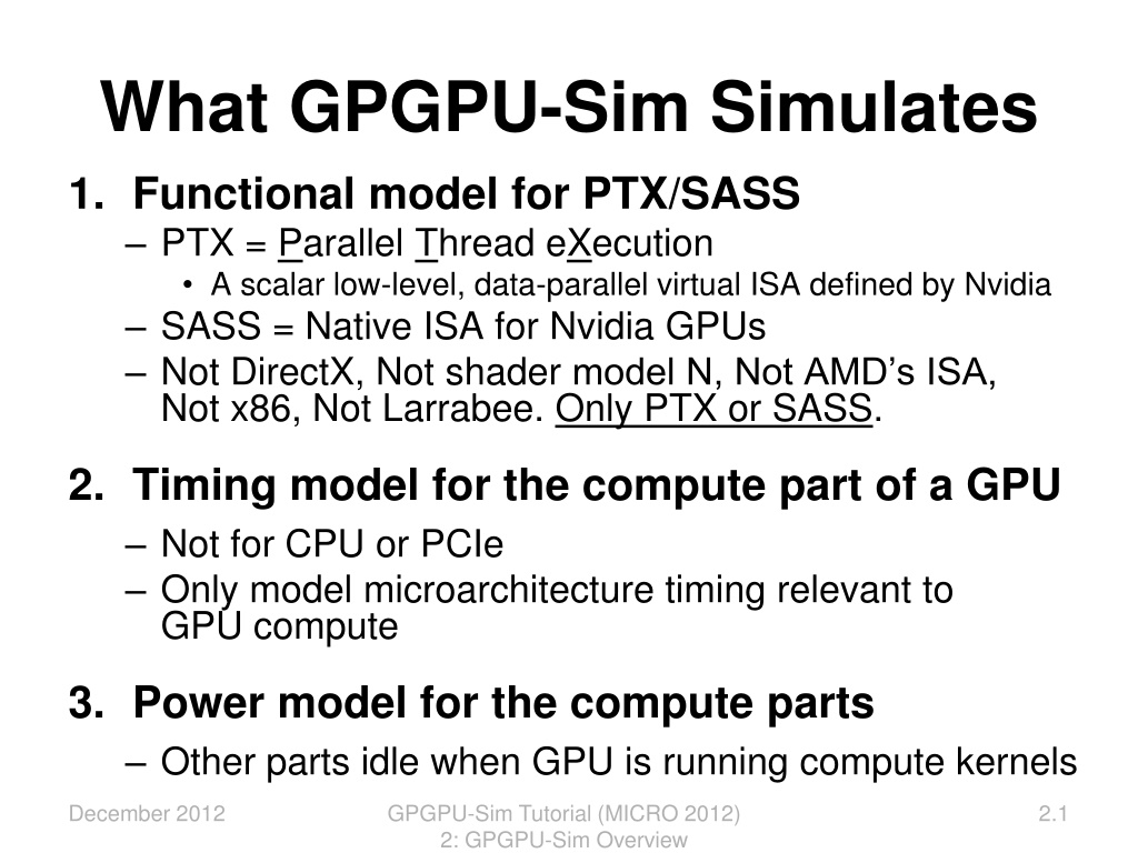
What GPGPU-Sim Simulates 1. Functional model for PTX/SASS PTX = Parallel Thread eXecution A scalar low-level, data-parallel virtual ISA defined by Nvidia SASS = Native ISA for Nvidia GPUs Not DirectX, Not shader model N, Not AMD s ISA, Not x86, Not Larrabee. Only PTX or SASS. 2. Timing model for the compute part of a GPU Not for CPU or PCIe Only model microarchitecture timing relevant to GPU compute 3. Power model for the compute parts Other parts idle when GPU is running compute kernels December 2012 GPGPU-Sim Tutorial (MICRO 2012) 2: GPGPU-Sim Overview 2.1
Functional Model (PTX) Low-level, data-parallel virtual machine by Nvidia Instruction level Unlimited registers Parallel threads running in blocks; barrier synchronization instruction Scalar ISA SIMT execution model Intermediate representation in CUDA tool chain: G80 GT200 Fermi Kepler .cu NVCC PTX ptxas .cl OpenCL Drv December 2012 GPGPU-Sim Tutorial (MICRO 2012) 2: GPGPU-Sim Overview 2.2
Functional Model (PTX) // some initialization code omitted $Lt_0_6146: bar.sync setp.le.s32 @%p3 bra ld.shared.f32 add.s32 cvt.s64.s32 mul.lo.u64 add.u64 ld.shared.f32 setp.gt.f32 @!%p4 bra st.shared.f32 $Lt_0_6914: $Lt_0_6402: shr.s32 mov.s32 and.b32 add.s32 shr.s32 mov.u32 setp.gt.s32 @%p5 bra for (int d = blockDim.x; d > 0; d /= 2) { __syncthreads(); 0; %p3, %r7, %r1; $Lt_0_6402; %f3, [%rd9+0]; %r9, %r7, %r1; %rd18, %r9; %rd19, %rd18, 4; %rd20, %rd6, %rd19; %f4, [%rd20+0]; %p4, %f3, %f4; $Lt_0_6914; [%rd9+0], %f4; if (tid < d) { float f0 = shared[tid]; float f1 = shared[tid + d]; if (f1 < f0) shared[tid] = f1; } } %r13, %r12, %r7; %r7, %r13, 1; %r14, 0; %p5, %r7, %r14; $Lt_0_6146; %r10, %r7, 31; %r11, 1; %r12, %r10, %r11; Scalar PTX ISA Scalar control flow (if-branch, for-loops) Parallel Intrinsic (__syncthreads()) Register allocation not done in PTX December 2012 GPGPU-Sim Tutorial (MICRO 2012) 2: GPGPU-Sim Overview 2.3
Interfacing GPGPU-Sim to Applications GPGPU-Sim compiles into a shared runtime library and implements the API: libcudart.so CUDA runtime API libOpenCL.so OpenCL API Static Linking no longer supported. Modify your LD_LIBRARY_PATH to run your CUDA app on GPGPU-Sim (See Manual) Need a config file (gpgpusim.config), an interconnection config file and a McPAT config as well We provide the config files for modeling: - Quadro FX 5800 (GT200) - Geforce GTX 480 and Tesla C2050 (Fermi) December 2012 GPGPU-Sim Tutorial (MICRO 2012) 2: GPGPU-Sim Overview 2.4
GPGPU-Sim Runtime Flow CUDA 3.1 CUDA 4.0 and Later December 2012 GPGPU-Sim Tutorial (MICRO 2012) 2: GPGPU-Sim Overview 2.5
Debugging and Visualization GPGPU-Sim provides tools to debug and visualize simulated GPU behavior. GDB macros: Cycle-level debugging AerialVision: High-level performance dynamics December 2012 GPGPU-Sim Tutorial (MICRO 2012) 2: GPGPU-Sim Overview 2.6
Timing Model for Compute Parts of a GPU Gfx DRAM GPGPU-Sim models timing for: SIMT Core (SM, SIMD Unit) Caches (Texture, Constant, ) Interconnection Network Memory Partition Graphics DRAM It does NOT model timing for: CPU, PCIe Graphics Specific HW (Rasterizer, Clipping, Display etc.) GPU Interconnect Cache Mem Part. SIMT Cores Gfx HW Raster PCIe CPU December 2012 GPGPU-Sim Tutorial (MICRO 2012) 2: GPGPU-Sim Overview 2.7
Timing Model for GPU Micro-architecture GPGPU-Sim simulates the timing model of a GPU running each launched CUDA kernel. Reports # cycles spent running the kernels. Exclude any time spent on data transfer on PCIe bus. CPU may run concurrently with asynchronous kernel launches. CPU Async. Kernel Launch GPU HW GPGPU-Sim Done GPU HW GPGPU-Sim Blocking Done CPU Sync. Kernel Launch GPU HW GPGPU-Sim Done CPU Time 2.8 December 2012 GPGPU-Sim Tutorial (MICRO 2012) 2: GPGPU-Sim Overview
Timing Model for GPU Micro-architecture GPGPU-Sim is a detailed cycle-level simulator: Cycle-level model for each part of the microarchitecture Research focused Ignoring rare corner cases to reduce complexity CUDA manual provides some hints. NVIDIA IEEE Micro articles provide other hints. In most cases we can only guess at details. Guesses informed by studying patents and microbenchmarking. GPGPU-Sim w/ SASS is ~0.98 correlated to the real HW. December 2012 GPGPU-Sim Tutorial (MICRO 2012) 2: GPGPU-Sim Overview 2.9
Timing Model Overview What is a warp? SIMT Core Internals SIMT Frontend Memory Unit Interconnection Network Clock Domains Memory Partition DRAM Timing Model December 2012 GPGPU-Sim Tutorial (MICRO 2012) 4: Microarchitecture Model 4.10
Thread Hierarchy Revisited Recall, kernel = grid of blocks of warps of threads Thread blocks (CTAs) contains up to 1024 threads Threads are grouped into warps in hardware Source: NVIDIA Each block is dispatched to a SIMT core as a unit of work: All of its warps run in the core s pipeline until they are all done. SIMT Core 32 Threads 32 Threads 32 Threads Thread Block (CTA) (CTA) (CTA) 32 Threads 32 Threads 32 Threads Thread Block Thread Block 32 Threads 32 Threads 32 Threads Warps December 2012 GPGPU-Sim Tutorial (MICRO 2012) 4: Microarchitecture Model 4.11
Warp = SIMT Execution of Scalar Threads Warp = Scalar threads grouped to execute in lockstep SIMT vs SIMD SIMD: HW pipeline width must be known by SW SIMT: Pipeline width hidden from SW ( ) Thread Warp 3 Thread Warp 8 Common PC Thread Warp Scalar Thread W Thread Warp 7 Scalar Thread X Scalar Thread Y Scalar Thread Z SIMT Pipeline ( ) Can still write software that assumes threads in a warp execute in lockstep (e.g. see reduction in NVIDIA SDK) December 2012 GPGPU-Sim Tutorial (MICRO 2012) 4: Microarchitecture Model 4.12
GPU Microarchitecture Overview GPU SIMT Core Cluster SIMT Core Cluster SIMT Core Cluster SIMT Core SIMT Core SIMT Core SIMT Core SIMT Core SIMT Core Interconnection Network Memory Partition Memory Partition Memory Partition Off-chip DRAM GDDR3/GDDR5 GDDR3/GDDR5 GDDR3/GDDR5 December 2012 GPGPU-Sim Tutorial (MICRO 2012) 4: Microarchitecture Model 4.13
Inside a SIMT Core Done (Warp ID) SIMT Front End Fetch Decode Schedule Branch Reg File SIMD Datapath Memory Subsystem SMem L1 D$ Tex $ Const$ Icnt. Network Fine-grained multithreading Interleave warp execution to hide latency Register values of all threads stays in core December 2012 GPGPU-Sim Tutorial (MICRO 2012) 4: Microarchitecture Model 4.14
Inside a SIMT Core (2.0) Schedule + Fetch Register Read Decode Execute Memory Writeback Started from a 5-stage In-Order Pipeline Add fine-grained multithreading Add SIMT stacks December 2012 GPGPU-Sim Tutorial (MICRO 2012) 4: Microarchitecture Model 4.15
Inside a SIMT Core (3.0) SIMT Front End SIMD Datapath Branch Target PC Fetch SIMT-Stack ALU ALU ALU ALU Scheduler 1 Scheduler 3 Valid[1:N] Active Mask Pred. I-Buffer Operand Collector I-Cache Decode Issue Score Board Scheduler 2 MEM Done (WID) Redesign Model Three decoupled warp schedulers Scoreboard Operand collector Multiple SIMD functional unit December 2012 GPGPU-Sim Tutorial (MICRO 2012) 4: Microarchitecture Model 4.16
Fetch + Decode Arbitrate the I-cache among warps Cache miss handled by fetching again later Fetched instruction is decoded and then stored in the I-Buffer 1 or more entries / warp Only warp with vacant entries are considered in fetch Score- Board Decode PC1 PC2 PC3 A R B v v v Inst. W1 r Inst. W2 Inst. W3 r r To I-Cache Selection To Fetch Issue ARB Issue Valid[1:N] Fetch Valid[1:N] I-Buffer I-Cache Decode December 2012 GPGPU-Sim Tutorial (MICRO 2012) 4: Microarchitecture Model 4.17
Instruction Issue Select a warp and issue an instruction from its I-Buffer for execution Round-Robin Priority GT200 (e.g. Quadro FX 5800): Allow dual issue Fermi: Odd/Even scheduler For each issued instruction: Functional execution Obtain info from functional simulator Generate coalesced memory accesses Reserve output register in scoreboard Update SIMT stack Score- Board Decode v v v Inst. W1 r Inst. W2 Inst. W3 r r To Fetch Issue ARB Issue December 2012 GPGPU-Sim Tutorial (MICRO 2012) 4: Microarchitecture Model 4.18
Scoreboard Checks for RAW and WAW dependency hazard Flag instructions with hazards as not ready in I-Buffer (masking them out from the scheduler) Instructions reserves registers at issue Release them at writeback December 2012 GPGPU-Sim Tutorial (MICRO 2012) 4: Microarchitecture Model 4.19
SIMT Stack foo[] = {4,8,12,16}; One stack per warp SIMT Stack A: v = foo[tid.x]; T1T2T3T4 A B: if (v < 10) PC RPC Active Mask T1T2T3T4 B B E - - 1111 1111 C: v = 0; T1T2 C D C E E 0011 1100 else T3T4 D D: v = 10; E: w = bar[tid.x]+v; T1T2T3T4 E Time Handles Branch Divergence December 2012 GPGPU-Sim Tutorial (MICRO 2012) 4: Microarchitecture Model 4.20
Operand Collector Bank 0 Bank 1 Bank 2 Bank 3 R0 R4 R8 R1 R5 R9 R2 R6 R10 R3 R7 R11 add.s32 R3, R1, R2; No Conflict mul.s32 R3, R0, R4; Conflict at bank 0 Operand Collector Architecture (US Patent: 7834881) Interleave operand fetch from different threads to achieve full utilization December 2012 GPGPU-Sim Tutorial (MICRO 2012) 4: Microarchitecture Model 4.21
Operand Collector (from instruction issue stage) dispatch December 2012 GPGPU-Sim Tutorial (MICRO 2012) 4: Microarchitecture Model 4.22
ALU Pipelines SIMD Execution Unit Fully Pipelined Each pipe may execute a subset of instructions Configurable bandwidth and latency (depending on the instruction) Default: SP + SFU pipes December 2012 GPGPU-Sim Tutorial (MICRO 2012) 4: Microarchitecture Model 4.23
Writeback Each pipeline has a result bus for writeback Exception: SP and SFU pipe shares a result bus Time slots on the shared bus is pre-allocated December 2012 GPGPU-Sim Tutorial (MICRO 2012) 4: Microarchitecture Model 4.24
Memory Unit Model timing for memory instructions Support half-warp (16 threads) Double clock the unit Each cycle service half the warp Has a private writeback path Bank Conflict Shared Mem MSHR Access Coalesc. Data Cache A G U Memory Port Const. Cache Texture Cache December 2012 GPGPU-Sim Tutorial (MICRO 2012) 4: Microarchitecture Model 4.25
Constant Cache A Read-only cache for constant memory GPGPU-Sim simulates 1 read ports A warp can access 1 constant cache locations in a single memory unit cycle If more than 1 locations accessed reads are serialized causing pipeline stalls # of ports is not configurable December 2012 GPGPU-Sim Tutorial (MICRO 2012) 4: Microarchitecture Model 4.26
Texture Cache Read-only cache with FIFO retirement Design based on Igehy et al. Prefetching in a Texture Cache Architecture, SIGGRAPH 1998. GPGPU-Sim support 1-D and 2-D textures 2-D locality should be preserved when texture cache blocks are fetched from memory GPGPU-Sim uses a 4-D blocking address scheme to promote spatial locality in 2-D Based on Hakura et al. The Design and Analysis of a Cache Architecture for Texture Mapping, ISCA 1997 December 2012 GPGPU-Sim Tutorial (MICRO 2012) 4: Microarchitecture Model 4.27
Shared Memory Explicitly managed scratchpad memory As fast as register files in absence of bank conflicts Threads in a block can cooperate via shared memory Each SIMT core has its own shared memory Dynamically allocated to thread blocks 16kB/48kB per SIMT core in current NVIDIA GPUs (Fermi) December 2012 GPGPU-Sim Tutorial (MICRO 2012) 4: Microarchitecture Model 4.28
Shared Memory (cont.) Many threads accessing memory Therefore Shared memory is highly banked Each bank serves one address per cycle Multiple access to a bank in a single cycle cause bank conflicts Conflicting accesses must be serialized Shared memory in NVIDIA GPUs has 16/32 banks Configurable in GPGPU-Sim (version 3.1.2) December 2012 GPGPU-Sim Tutorial (MICRO 2012) 4: Microarchitecture Model 4.29
Shared Memory Bank Conflicts Figures taken from CUDA manual by NVIDIA No bank conflict 8-way bank conflict December 2012 GPGPU-Sim Tutorial (MICRO 2012) 4: Microarchitecture Model 4.30
Global Memory Global memory is the off-chip DRAM memory The largest and slowest memory available Accesses must go through interconnect, memory partition and off-chip DRAM Optionally cached in HW L1 Data Cache L2 Unified Cache December 2012 GPGPU-Sim Tutorial (MICRO 2012) 4: Microarchitecture Model 4.31
Coalescing Combining memory accesses made by threads in a warp into fewer transactions E.g. if threads in a warp are accessing consecutive 4-byte sized locations in memory Send one 128 byte request to DRAM (coalescing) Instead of 32 4-byte requests This reduces the number of transactions between SIMT cores and DRAM Less work for Interconnect, Memory Partition and DRAM December 2012 GPGPU-Sim Tutorial (MICRO 2012) 4: Microarchitecture Model 4.32
Coalescing (Cont.) CUDA Capability 1.3 (e.g. GTX280) Coalescing done per half-warp Can create 128-byte, 64-byte or 32-byte transactions CUDA Capability 2.0 (e.g. Fermi) Coalescing done for a full warp Cached: Only creates 128-byte transactions Not Cached: Can create 128/64/32-byte transactions GPGPU-Sim supports both December 2012 GPGPU-Sim Tutorial (MICRO 2012) 4: Microarchitecture Model 4.33
Coalescing (cont.) Coalescing example = 4-bytes in memory Figures taken from CUDA manual by NVIDIA One 128-Byte Transaction Warp Two 128-Byte Transactions Warp December 2012 GPGPU-Sim Tutorial (MICRO 2012) 4: Microarchitecture Model 4.34
L1 Data Cache For both local and global memory space With different policies Local Memory Write Hit Write-back Write Miss Write no-allocate Global Memory Write-evict Write no-allocate Non-coherent Single ported (128-Byte wide) Takes multiple cycles to service non-coalesced accesses December 2012 GPGPU-Sim Tutorial (MICRO 2012) 4: Microarchitecture Model 4.35
Memory Access Tracking Cached access Miss Status Holding Registers (MSHR) Non-cached access Encode warp, target register in request packet Memory Unit writes replied data directly to target request December 2012 GPGPU-Sim Tutorial (MICRO 2012) 4: Microarchitecture Model 4.36
Miss Status Holding Registers MSHRs keep track of outstanding memory requests keep track of threads, target registers, request addresses GPGPU-Sim: Each cache has its set of MSHRs Each MSHR contains one or more memory requests to the same address MSHRs are limited (configurable) Memory unit stalls if cache runs out of MSHRS One approach that might make sense No details available from NVIDIA / AMD December 2012 GPGPU-Sim Tutorial (MICRO 2012) 4: Microarchitecture Model 4.37
Atomic Operations Both CUDA and OpenCL support atomic operations Read-modify-write on a single memory location Coalescing rules ~ global memory access Put accesses to same memory location in separate transactions GPGPU-Sim simulate these as: Load operations inside a SIMT core Skips L1 data cache Store operations at memory partition December 2012 GPGPU-Sim Tutorial (MICRO 2012) 4: Microarchitecture Model 4.38
SIMT Core Model (Fermi Architecture) Just a configuration in our model December 2012 GPGPU-Sim Tutorial (MICRO 2012) 4: Microarchitecture Model 4.39
SIMT Core Cluster Collection of SIMT cores December 2012 GPGPU-Sim Tutorial (MICRO 2012) 4: Microarchitecture Model 4.40
GPU Microarchitecture Overview GPU SIMT Core Cluster SIMT Core Cluster SIMT Core Cluster SIMT Core SIMT Core SIMT Core SIMT Core SIMT Core SIMT Core Interconnection Network Memory Partition Memory Partition Memory Partition Off-chip DRAM GDDR3/GDDR5 GDDR3/GDDR5 GDDR3/GDDR5 December 2012 GPGPU-Sim Tutorial (MICRO 2012) 4: Microarchitecture Model 4.41
Clock domains Simulate independent clock domains for SIMT cores GT200: Set to of shader clock to compensate for using SIMD width of 32 instead of 8 Fermi: Set to of shader clock to compensate for using SIMD width of 32 instead of 16 Interconnection network L2 cache (if enabled) DRAM This is real clock (command clock) Effective clock is 2x this clock due to DDR December 2012 GPGPU-Sim Tutorial (MICRO 2012) 4: Microarchitecture Model 4.42
Clock Domain Crossing We simulate send and receive buffers at clock crossing boundaries The buffers are filled and drained in different clock domains E.g. consider the buffer from interconnect to memory partition Filled at interconnect clock rate Drained at DRAM clock rate December 2012 GPGPU-Sim Tutorial (MICRO 2012) 4: Microarchitecture Model 4.43
Interconnection Network Model Intersim (Booksim) a flit level simulator Topologies (Mesh, Torus, Butterfly, ) Routing (Dimension Order, Adaptive, etc. ) Flow Control (Virtual Channels, Credits) We simulate two separate networks From SIMT cores to memory partitions Read Requests, Write Requests From memory partitions to SIMT cores Read Replies, Write Acks December 2012 GPGPU-Sim Tutorial (MICRO 2012) 4: Microarchitecture Model 4.44
Topology Examples December 2012 GPGPU-Sim Tutorial (MICRO 2012) 4: Microarchitecture Model 4.45
Interconnection Network Config Booksim has its own config file Topology (topology, k ,n ) Virtual channels (num_vcs) Buffers per VC (vc_buf_size) Routing (routing _function) Speedups (input_speedup, internal_speedup) Allocators (vc_allocator, sw_allocator) Specific to GPGPU-sim Channel Width (flit_size) Setting memory partition locations (use_map) December 2012 GPGPU-Sim Tutorial (MICRO 2012) 4: Microarchitecture Model 4.46
Interconnect Injection Interfaces 1 Flit / Cycle 1 Packet / Cycle SIMT Core Router Core Clock Domain Interconnect Clock Domain Clock Boundary December 2012 GPGPU-Sim Tutorial (MICRO 2012) 4: Microarchitecture Model 4.47
Interconnect Injection Interfaces 1 Flit / Cycle 1 Packet / Cycle Memory Partition Router DRAM Clock Domain Interconnect Clock Domain Clock Boundary December 2012 GPGPU-Sim Tutorial (MICRO 2012) 4: Microarchitecture Model 4.48
Interconnect Injection Interfaces 1 Flit / Cycle 1 Packet / Cycle L2 Router Cache L2 Clock Domain Interconnect Clock Domain Clock Boundary December 2012 GPGPU-Sim Tutorial (MICRO 2012) 4: Microarchitecture Model 4.49
Interconnect Ejection Interfaces 1 Ejection/boundary buffer per VC (1 flit / cycle) A credit is sent back to router as a flit goes from ejection to boundary buffer # of VCs 1 Packet / Cycle (Round Robin) 1 Flit / Cycle Boundary Buffers Ejection Buffers 1 Flit / Cycle SIMT Core Router 1 Credit / Cycle Credit return buffer Interconnect Clock Domain Core Clock Domain Clock Boundary December 2012 GPGPU-Sim Tutorial (MICRO 2012) 4: Microarchitecture Model 4.50

")
")


")
")


")


")
")


