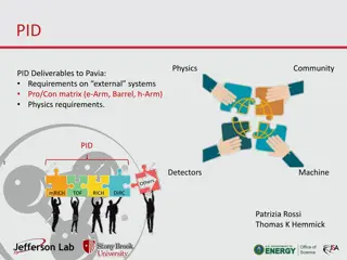
Gated Mode Systems in Particle Detectors


Gated Mode - System Aspects
F
e
l
i
x
M
ü
l
l
e
r
o
n
b
e
h
a
l
f
o
f
t
h
e
G
a
t
e
d
M
o
d
e
c
r
e
w
(
C
h
r
i
s
t
i
a
n
K
o
f
f
m
a
n
e
,
P
h
i
l
i
p
p
L
e
i
t
l
,
L
u
i
g
i
L
i
G
i
o
i
)


21
st
International Workshop on DEPFET
Detectors and Applications
28
th
– 31
th
May 2017
Ringberg Castle
Gated Mode - Theory
•
Continuous top-up injection with 50 Hz, i.e., every 20 ms
•
Bunch revolution time: 10 μs
•
Shield detector during passing of noisy bunches
•
Limit by other sub-detectors: 1 μs
•
BEAST Phase 2 will bring more information about damping time
KEKB
Gated Mode
10 µs
Dead time:
1.4 µs – 1.9 µs
→
14% of sensitive area
→
19% of sensitive area
readout
direction
20 µs
Gated Mode
Gated Mode
PXD sensitive area
D
e
a
d
t
i
m
e
:
S
h
i
e
l
d
i
n
g
o
f
D
E
P
F
E
T
s
a
n
d
P
e
d
e
s
t
a
l
o
s
c
i
l
l
a
t
i
o
n
s
/
r
e
l
a
x
a
t
i
o
n
DHP – DCD – Switcher principle
gate i
gate i+1
gate i+2
gate 192
gate 1
spare until
gate 256
from
DCD
to
DCD
128bit to
Switcher
<, >
threshold
gate changes every 8
clock cycles of GCK
512
512
normal
VETO
DHP memory blocks
DHP – DCD – Switcher principle for GM
gate i
gate changes every
8 clock cycles of
GCK
gate i+1
gate i+k
gate i+k+1
Normal sequence
Switcher sequence
G
M
Gated Mode
•
Apply Clear On voltage at all DEPFET pixels
•
Switch Off the DEPFET
•
192 Switcher outputs in total
•
Four groups to (de)-activate the Gated Mode, each Switcher has 4 groups:
•
Each Switcher (de)-activate the Gated Mode for 8 gates simultaneously
Gated Mode w/o readout
Stop Readout
During gating there is no readout
Continue readout after gating
need to be in sync with offsets,
pedestals and machine => Fast
clocking
Gated Mode w/o readout
Fast
clocking to
get in sync
Gated Mode w/o readout
“Missing next frame” (Missing all frames
during the damping time of noisy
bunches (which prevent the sampling of
the SerIn signal)) problem
Switcher requires high clock for SerIn
Gated Mode w/o readout
Advantages
:
•
Can ramp up/down the Switcher groups with steps of 7.56 ns
•
Adjust the length of activating the GM in steps of 3.26 ns
•
Fast (de)-activation: 20 ns in theory for (de)-activation, and (90 ns) 75 ns are measured
Disadvantage(s)
:
•
Missing “next frame” problem / Missing all frames during the damping time of noisy bunches (which
prevent the sampling of the SerIn signal)
I
n
a
d
d
i
t
i
o
n
:
P
e
d
e
s
t
a
l
o
s
c
i
l
l
a
t
i
o
n
,
i
.
e
.
,
r
e
q
u
i
r
e
e
x
t
r
a
t
i
m
e
f
o
r
r
e
l
a
x
a
t
i
o
n
o
f
p
e
d
e
s
t
a
l
s
,
~
1
µ
s
(
m
u
s
t
b
e
m
e
a
s
u
r
e
d
a
g
a
i
n
i
n
m
o
r
e
d
e
t
a
i
l
w
i
t
h
n
e
w
e
s
t
g
e
n
e
r
a
t
i
o
n
o
f
A
S
I
C
s
)
•
t
o
t
a
l
t
i
m
e
f
o
r
G
M
:
~
3
7
0
n
s
•
t
o
t
a
l
G
a
t
e
d
M
o
d
e
(
e
n
a
b
l
i
n
g
,
g
a
t
i
n
g
,
d
i
s
a
b
l
i
n
g
,
t
i
m
e
t
o
n
o
r
m
a
l
o
p
e
r
a
t
i
o
n
)
:
1
.
4
µ
s
Gated Mode without readout
W
3
7
-
I
B
Felix Müller, Christian Koffmane
Switcher substrate
voltage
DHPT 1.1
DCDBv4.2
SWB18v2.1
Ideas to solve problems – pedestal oscillations
1) Stop GCK after switching back to normal mode for 1
μ
s
•
ensure synchronization with offsets and pedestals
•
Extend readout time from 20
μ
s to 22
μ
s
~1
μ
s
GCK
20
μ
s
40
μ
s
60
μ
s
0
μ
s
80
μ
s
Normal
readout
Gated
Mode
Is it possible from DHE, DHP?
Gated Mode
Ideas to solve problems – pedestal oscillations
2
)
R
u
n
n
i
n
g
G
C
K
,
s
t
o
p
S
w
i
t
c
h
e
r
s
e
q
u
e
n
c
e
Extend Switcher Sequence with empty signals,
i.e., stop continuous rolling shutter mode
•
out of sync with offsets
•
out of sync with pedestals (occupancy
↑
)
G
M
Matrix readout
Pedestals memory
D
o
e
s
n
o
t
w
o
r
k
FSYNC signal
DHP reads / writes data in the next memory line every 8 clock cycles
S
e
r
I
n
s
i
g
n
a
l
i
s
s
t
o
r
e
d
i
n
g
a
t
e
1
9
0
Problem if the Gated Mode without readout is applied during gate 190
192
1
F
S
Y
N
C
F
S
Y
N
C
r
e
s
e
t
s
a
l
l
m
e
m
o
r
y
p
o
i
n
t
e
r
s
(Switcher sequence, offsets, pedestals)
After 1536 clock cycles (8*192)
DHP memory
Ideas to solve problems – “missing next frame”
3) Extend Switcher sequence and build SerIn and CLK after normal GM sequence
normal GM
sequence
extended GM
sequence
extended GM sequence:
SerIn and
high
Clock
Question: How fast can we write to
JTAG that DHP should read SerIn from
VETO Switcher Sequence?
DHPT1.2 allows to decide whether the SerIn is used from normal
switcher sequence or from Gated Mode switcher sequence:
configuration via JTAG command
D
H
E
n
e
e
d
s
t
o
s
e
n
t
t
h
e
F
S
Y
N
C
m
o
r
e
t
h
a
n
1
5
3
6
c
l
o
c
k
c
y
c
l
e
s
.
O
t
h
e
r
w
i
s
e
t
h
e
m
e
m
o
r
y
p
o
i
n
t
e
r
w
i
t
h
i
n
t
h
e
D
H
P
i
s
r
e
s
e
t
.
Does the DHE allow variable lengths of FSYNC for one frame?
At least two fixed lengths?
DHP memory
Ideas to solve problems – “missing next frame”
3) Extend Switcher sequence and build SerIn and CLK after normal GM sequence
•
Keep in sync with pedestals, offsets
•
Out of sync with machine – Problems?
20
μ
s
40
μ
s
60
μ
s
0
μ
s
80
μ
s
Normal
readout
Gated
Mode
Gated Mode
SerIn
Gated Mode with readout
•
Continue readout during Gated Mode
•
Cannot read DEPFET values due to pedestal oscillations
•
Need 315 ns for (de)-activation in theory (20 ns for GM without readout)
•
Measured 330 ns / 335 ns for (de)-activation in practice
•
Adjust shielding time in steps of 105 ns (3.27 ns for GM without readout)
Gated Mode with readout
W
3
7
-
I
B
Felix Müller, Christian Koffmane
Switcher substrate
voltage
DHPT 1.1
DCDBv4.2
SWB18v2.1
Group 1
Group 2
Group 3
Group 4
Group 1
Group 2
Group 3
Group 4
Gated Mode – 2 Possibilities
G
a
t
e
d
M
o
d
e
w
i
t
h
r
e
a
d
o
u
t
(
G
M
w
/
R
O
)
:
•
needs 315 ns in theory (330 ns measured) to enable the GM, i.e., to shield all pixels
•
needs 315 ns in theory (335 ns measured) to disable the GM, i.e., to switch to normal operation
•
can apply the GM for all pixels in steps of 105 ns
•
t
o
t
a
l
t
i
m
e
f
o
r
G
M
:
~
8
7
0
n
s
•
additionally, the read-out of the pedestals currents after the GM show oscillations (increased
spread), which take ~ 1µs (
must be measured again in more detail
)
•
t
o
t
a
l
G
a
t
e
d
M
o
d
e
(
e
n
a
b
l
i
n
g
,
g
a
t
i
n
g
,
d
i
s
a
b
l
i
n
g
,
t
i
m
e
t
o
n
o
r
m
a
l
o
p
e
r
a
t
i
o
n
)
:
1
.
6
µ
s
–
1
.
9
µ
s
G
a
t
e
d
M
o
d
e
w
i
t
h
o
u
t
r
e
a
d
o
u
t
(
G
M
w
/
o
R
O
)
:
•
needs 20 ns in theory (75 ns measured) to enable the GM, i.e., to shield all pixels
•
needs 20 ns in theory (90 ns measured) to disable the GM, i.e., to switch to normal operation
•
can apply the GM for all pixels in steps of 3.27 ns
•
t
o
t
a
l
t
i
m
e
f
o
r
G
M
:
~
3
7
0
n
s
•
additional pedestals currents after the GM : ~1 µs (
must be measured again in more detail
)
•
t
o
t
a
l
G
a
t
e
d
M
o
d
e
(
e
n
a
b
l
i
n
g
,
g
a
t
i
n
g
,
d
i
s
a
b
l
i
n
g
,
t
i
m
e
t
o
n
o
r
m
a
l
o
p
e
r
a
t
i
o
n
)
:
1
.
4
µ
s
Measurements on W37-IB (PXD9-7 with SWB18v2.1)
Felix Müller, Christian Koffmane
Layout change – PXD9-7
Reduced ohmic resistance from Switcher Substrate net
PXD9-6: 55
Ω
for Switcher 1, 172
Ω
for Switcher 6
PXD9-7: 10
Ω
for Switcher 1, 27
Ω
for Switcher 6
W
3
1
-
O
F
1
DHPT 1.1
DCDBv4.2
SWB18v2.
0
Layout change – PXD9-7
Reduced ohmic resistance from Switcher Substrate net
PXD9-6: 55
Ω
for Switcher 1, 172
Ω
for Switcher 6
PXD9-7: 10
Ω
for Switcher 1, 27
Ω
for Switcher 6
W
3
1
-
O
F
1
DHPT 1.1
DCDBv4.2
SWB18v2.
0
Summary and Outlook
•
Gated Mode without readout is faster but there is the “missing next frames” problem
Ideas to shift frame, increase frame time – need to consider system aspects
from DHE/DHP
•
Need to measure pedestal oscillation time
•
Testing procedures for GM mass testing to be evaluated if needed?
•
Wait after “mass testing”
•
I
s
i
t
b
e
t
t
e
r
t
o
u
s
e
G
M
w
/
o
R
O
a
n
d
l
o
s
e
i
n
1
.
6
%
o
f
t
h
e
c
a
s
e
s
t
h
e
4
m
s
(
2
0
0
f
r
a
m
e
s
)
w
i
t
h
g
a
t
i
n
g
t
i
m
e
o
f
1
.
4
µ
s
O
R
is it better to use GM w/ RO, do not lose consecutive frames but with a gating time of
1.9 µs (preliminary)
⇒
P
l
a
n
n
e
d
:
E
f
f
e
c
t
o
f
t
h
e
P
X
D
G
a
t
e
d
M
o
d
e
o
n
P
h
y
s
i
c
s
s
h
o
u
l
d
b
e
e
v
a
l
u
a
t
e
d
Radioactive Source and Laser setup
•
Infrared Laser (980 nm) to cover entire module area
•
Needs to be installed (Laser safety 3B)
•
LED setup to study clear efficiencies and gated mode operation, not in pixel
scan, no laser setup
Felix Müller, 14.09.2016 - 10th Belle II VXD Workshop
Readout directions (1)
L2 BWD
L2
F
WD
L1 BWD
L1 FWD
Felix Müller, Christian Koffmane
Arrows depict the readout direction
Readout directions (2)
Backward
Forward
Arrows depict the readout direction
Felix Müller, Christian Koffmane
PXD Arrangement
Arrows depict the readout direction
Felix Müller, Christian Koffmane
Delve into the intricate details of Gated Mode systems, focusing on aspects such as theory, sensitivity areas, switcher principles, and readout processes without compromising data integrity. Explore the challenges and strategies involved in implementing Gated Mode technology effectively in DEPFET detectors for particle applications.

Download Presentation

Please find below an Image/Link to download the presentation.
The content on the website is provided AS IS for your information and personal use only. It may not be sold, licensed, or shared on other websites without obtaining consent from the author.If you encounter any issues during the download, it is possible that the publisher has removed the file from their server.
You are allowed to download the files provided on this website for personal or commercial use, subject to the condition that they are used lawfully. All files are the property of their respective owners.
The content on the website is provided AS IS for your information and personal use only. It may not be sold, licensed, or shared on other websites without obtaining consent from the author.
E N D
Presentation Transcript
Gated Mode - System Aspects Felix M ller on behalf of the Gated Mode crew (Christian Koffmane, Philipp Leitl, Luigi Li Gioi) 21st International Workshop on DEPFET Detectors and Applications 28th 31th May 2017 Ringberg Castle 1
Gated Mode - Theory KEKB Continuous top-up injection with 50 Hz, i.e., every 20 ms Bunch revolution time: 10 s Shield detector during passing of noisy bunches Limit by other sub-detectors: 1 s BEAST Phase 2 will bring more information about damping time 2
Gated Mode PXD sensitive area readout direction Dead time: 1.4 s 1.9 s Gated Mode 20 s 14% of sensitive area 19% of sensitive area 10 s Gated Mode Dead time: Shielding of DEPFETs and Pedestal oscillations / relaxation 3
DHP DCD Switcher principle gate changes every 8 clock cycles of GCK DHP memory blocks Switcher Switcher Signal Pedestal Offset gate 1 <, > to 512 128bit to from gate i threshold DCD Switcher DCD gate i+1 gate i+2 gate 192 spare until gate 256 512 4
DHP DCD Switcher principle for GM gate changes every 8 clock cycles of Switcher Signal Pedestal Offset GCK gate i GM Normal sequence gate i+k+1 gate i+1 gate i+k Switcher sequence 5
Gated Mode Apply Clear On voltage at all DEPFET pixels Switch Off the DEPFET 192 Switcher outputs in total Four groups to (de)-activate the Gated Mode, each Switcher has 4 groups: Each Switcher (de)-activate the Gated Mode for 8 gates simultaneously 6
Gated Mode w/o readout Stop Readout During gating there is no readout Continue readout after gating need to be in sync with offsets, pedestals and machine => Fast clocking 7
Gated Mode w/o readout Fast clocking to get in sync 8
Gated Mode w/o readout Missing next frame (Missing all frames during the damping time of noisy bunches (which prevent the sampling of the SerIn signal)) problem Switcher requires high clock for SerIn 9
Gated Mode w/o readout Advantages: Can ramp up/down the Switcher groups with steps of 7.56 ns Adjust the length of activating the GM in steps of 3.26 ns Fast (de)-activation: 20 ns in theory for (de)-activation, and (90 ns) 75 ns are measured Disadvantage(s): Missing next frame problem / Missing all frames during the damping time of noisy bunches (which prevent the sampling of the SerIn signal) In addition: Pedestal oscillation, i.e., require extra time for relaxation of pedestals, ~ 1 s (must be measured again in more detail with newest generation of ASICs) total time for GM: ~ 370 ns total Gated Mode (enabling, gating, disabling, time to normal operation): 1.4 s 10
Gated Mode without readout W37-IB DHPT 1.1 DCDBv4.2 SWB18v2.1 Switcher substrate voltage 11 Felix M ller, Christian Koffmane
Ideas to solve problems pedestal oscillations 1) Stop GCK after switching back to normal mode for 1 s ensure synchronization with offsets and pedestals Extend readout time from 20 s to 22 s GCK ~1 s Gated Mode Normal readout Gated Mode 60 s 80 s 20 s 40 s 0 s Is it possible from DHE, DHP? 12
Ideas to solve problems pedestal oscillations Switcher Signal Pedestal Offset 2) Running GCK, stop Switcher sequence Extend Switcher Sequence with empty signals, i.e., stop continuous rolling shutter mode out of sync with offsets out of sync with pedestals (occupancy ) GM Matrix readout Pedestals memory 13
FSYNC signal DHP reads / writes data in the next memory line every 8 clock cycles SerIn signal is stored in gate 190 Problem if the Gated Mode without readout is applied during gate 190 FSYNC DHP memory 1 192 FSYNC resets all memory pointers (Switcher sequence, offsets, pedestals) After 1536 clock cycles (8*192) 14
Ideas to solve problems missing next frame 3) Extend Switcher sequence and build SerIn and CLK after normal GM sequence DHPT1.2 allows to decide whether the SerIn is used from normal switcher sequence or from Gated Mode switcher sequence: configuration via JTAG command DHP memory extended GM sequence: SerIn and high Clock normal GM sequence extended GM sequence Question: How fast can we write to JTAG that DHP should read SerIn from VETO Switcher Sequence? DHE needs to sent the FSYNC more than 1536 clock cycles. Otherwise the memory pointer within the DHP is reset. Does the DHE allow variable lengths of FSYNC for one frame? At least two fixed lengths? 15
Ideas to solve problems missing next frame 3) Extend Switcher sequence and build SerIn and CLK after normal GM sequence Keep in sync with pedestals, offsets Out of sync with machine Problems? Gated Mode Normal readout SerIn Gated Mode 60 s 80 s 20 s 40 s 0 s 16
Gated Mode with readout Continue readout during Gated Mode Cannot read DEPFET values due to pedestal oscillations Need 315 ns for (de)-activation in theory (20 ns for GM without readout) Measured 330 ns / 335 ns for (de)-activation in practice Adjust shielding time in steps of 105 ns (3.27 ns for GM without readout) 17
Gated Mode with readout W37-IB Group 1 Group 2 Group 3 Group 4 DHPT 1.1 DCDBv4.2 SWB18v2.1 Switcher substrate voltage Group 4 Group 3 Group 2 Group 1 18 Felix M ller, Christian Koffmane
Gated Mode 2 Possibilities Measurements on W37-IB (PXD9-7 with SWB18v2.1) Gated Mode with readout (GM w/ RO): needs 315 ns in theory (330 ns measured) to enable the GM, i.e., to shield all pixels needs 315 ns in theory (335 ns measured) to disable the GM, i.e., to switch to normal operation can apply the GM for all pixels in steps of 105 ns total time for GM: ~ 870 ns additionally, the read-out of the pedestals currents after the GM show oscillations (increased spread), which take ~ 1 s (must be measured again in more detail) total Gated Mode (enabling, gating, disabling, time to normal operation): 1.6 s 1.9 s Gated Mode without readout (GM w/o RO): needs 20 ns in theory (75 ns measured) to enable the GM, i.e., to shield all pixels needs 20 ns in theory (90 ns measured) to disable the GM, i.e., to switch to normal operation can apply the GM for all pixels in steps of 3.27 ns total time for GM: ~ 370 ns additional pedestals currents after the GM : ~1 s (must be measured again in more detail) total Gated Mode (enabling, gating, disabling, time to normal operation): 1.4 s 19 Felix M ller, Christian Koffmane
Layout change PXD9-7 Reduced ohmic resistance from Switcher Substrate net PXD9-6: 55 for Switcher 1, 172 for Switcher 6 PXD9-7: 10 for Switcher 1, 27 for Switcher 6 W31-OF1 DHPT 1.1 DCDBv4.2 SWB18v2.0 20
Layout change PXD9-7 Reduced ohmic resistance from Switcher Substrate net PXD9-6: 55 for Switcher 1, 172 for Switcher 6 PXD9-7: 10 for Switcher 1, 27 for Switcher 6 W31-OF1 DHPT 1.1 DCDBv4.2 SWB18v2.0 21
Summary and Outlook Gated Mode without readout is faster but there is the missing next frames problem Ideas to shift frame, increase frame time need to consider system aspects from DHE/DHP Need to measure pedestal oscillation time Testing procedures for GM mass testing to be evaluated if needed? Wait after mass testing Is it better to use GM w/o RO and lose in 1.6% of the cases the 4 ms (200 frames) with gating time of 1.4 s OR is it better to use GM w/ RO, do not lose consecutive frames but with a gating time of 1.9 s (preliminary) Planned: Effect of the PXD Gated Mode on Physics should be evaluated Gated Mode w/o RO Gated Mode w/ RO (De)activation 90 ns Adjustment of gating time in steps of 3.27 ns Total time for GM 370 ns + pedestal oscillations De(activation) needs 335 ns Adjustment of gating time in steps of 105 ns Total time for GM 870 ns + pedestal oscillations 22
Radioactive Source and Laser setup Infrared Laser (980 nm) to cover entire module area Needs to be installed (Laser safety 3B) LED setup to study clear efficiencies and gated mode operation, not in pixel scan, no laser setup 23 Felix M ller, 14.09.2016 - 10th Belle II VXD Workshop
Readout directions (1) L2 FWD L2 BWD Arrows depict the readout direction L1 BWD L1 FWD 24 Felix M ller, Christian Koffmane
Readout directions (2) Backward Forward Arrows depict the readout direction 25 Felix M ller, Christian Koffmane
PXD Arrangement Arrows depict the readout direction 26 Felix M ller, Christian Koffmane


")
")