Characteristics of Logic Families : I-V Requirements
Explore the voltage and current requirements for logic families, detailing the parameters for logic levels 1 and 0. Understand the significance of VIH, VIL, VOH, and VOL in maintaining proper logic functionality. This information is crucial for designing and implementing effective logic circuits.

Download Presentation

Please find below an Image/Link to download the presentation.
The content on the website is provided AS IS for your information and personal use only. It may not be sold, licensed, or shared on other websites without obtaining consent from the author.If you encounter any issues during the download, it is possible that the publisher has removed the file from their server.
You are allowed to download the files provided on this website for personal or commercial use, subject to the condition that they are used lawfully. All files are the property of their respective owners.
The content on the website is provided AS IS for your information and personal use only. It may not be sold, licensed, or shared on other websites without obtaining consent from the author.
E N D
Presentation Transcript
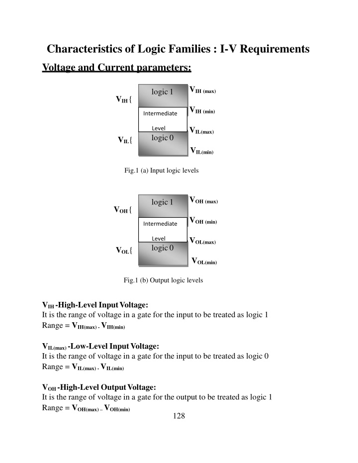
Characteristics of Logic Families : I-V Requirements Voltage and Current parameters: VIH (max) logic1 VIH{ VIH (min) Intermediate VIL(max) Level logic0 VIL{ VIL(min) Fig.1 (a) Input logic levels VOH (max) logic1 VOH{ VOH (min) Intermediate VOL(max) Level logic0 VOL{ VOL(min) Fig.1 (b) Output logic levels VIH -High-Level InputVoltage: It is the range of voltage in a gate for the input to be treated as logic 1 Range = VIH(max) -VIH(min) VIL(max) -Low-Level InputVoltage: It is the range of voltage in a gate for the input to be treated as logic 0 Range = VIL(max) -VIL(min) VOH -High-Level OutputVoltage: It is the range of voltage in a gate for the output to be treated as logic 1 Range = VOH(max) VOH(min) 128
VOL- Low Level Output Voltage: It is the range of voltage in a gate for the output to be treated as logic 0 Range = VOL(max) VOL(min) IIH - High Level InputCurrent: It is the current that flows in the input when voltage of VIH applied. range (logic1)is IIL- Low Level Input Current: It is the current that flows in the input when voltage of VIH applied. range (logic0)is IOH - High Level OutputCurrent: It is the current that flows from in the output when voltage of VOH is obtained under given load. range (logic1) IOL- Low Level Output Current: It is the current that flows from in the output when voltage of VOL is obtained under given load. range (logic0) Fig.2: Currents and voltages in the two logic states 129
Fan-in and Fan-out: Fan-in: the number of inputs of a gate that it can handle without impairing its normal operation. 1 2 3 Fan-in = number of inputs Propagation delay increases with number of inputs. Therefore a 2 input NAND gate is faster than 4 input NAND gate. Fan-out: The number of standard loads can be connected to the output of the gate without affecting its normal operation. Sometimes the term loading is used. Fig.3: fan-out computation 130
Fan out = min( IOH , IOL ) IIH IIL High state fan-out = IOH(max) IIH Low state fan-out = IOL(max) IIL For TTLgate: High state fan-out = 400 ?=10 40 ? Low state fan-out = 16mA =10 1.6mA Noise margin: -The unwanted signals are referred to as noise. - Noise margin is the maximum noise added to an input signal of a digital circuit that does not cause an undesirable change in the circuit output. Fig.4: Noisemargins 131
High state noise margin: V = V (min) V (min) OH NH IH Low state noise margin: V = V (max) V IL (max) OL NL Propagation delay: The average transition-delay time for the signal to propagate from input to output when the binary signal changes in value 1.tPLH : It is the delay time measured to logic 1 state (LOW to HIGH). when output is changing from logic 0 2.tPHL: It is the delay time measured when output is changing from logic 1 to logic 0 state (HIGH to LOW). When tPHL and tPLH are not equal, the larger value is considered as a propagation delay time for that logic gate,i.e. tp = max (tPLH,tPHL) Sometimes propagation delay tp is taken to be the simple average of the two : t = 1(t + t ) P PHL PLH 2 Figure 5 shows logic gates with different fan-outs and their corresponding propagation delays. 132
Fig.5: Fan-outs and corresponding propagation delays Power dissipation: -The power needed by the gate is expressed in mW. +ICCL 2 (avg) =ICCH I CC PD (avg) = ICC (avg) VCC Fig.6: Currents lCCH andICCL 133
Example 2: A certain gate draws 1.8 mA when its output is HIGH and 3.2 mA when its output is LOW. What is its average power dissipation if VCCis 5 V and it is operated on a 50 % duty cycle? Solution:The average Ice is given as, ICC(avg)=ICCH+ICCL = 2 = 2.5mA Then average power dissipation is given as, PD (avg) = ICC(avg) X VCC = 2.5 mA x 5 V = 12.5 mW Speed-power product(J)=Propagation delay (Seconds) x Power dissipation (joules/seconds) Example 3: For a certain IC family, propagation delay is 10 ns with an average power dissipation of 6 mW. What is its speed power product? Solution: The speed- power product is given as, SPP = Propagation delay x Average power dissipation = 10 ns x 6 mW x 60 pico joules (pJ) Example 4: If V cc = 5VCC= 5V, ICC (0) 22 mA, 1CC (1) = 8mA, VOH = 2.4 V, VIH=2 V, VOL = 0.45 V, VIL = 0.8 V, tPHL = 15nsec, tPLH = 22 nsec, IIH = 40?A, IOH = 5.2 mA. calculate : Noise margin logic 1 and logic 0. Power dissipation. Propagation delay and figure of merit. Fan-out. i) ii) iii) iv) 134
Solution: i) Noise margin logic 1 VNH = VOH(min) -VIH(min) = 2.4 V 2 V VNH = 0.4V Noise margin logic 0 VNL = VIL(max) VOL(max) = 0.8 V 0.45V VNL = 0.35V ii) Powerdissipation ICC(avg)XVCC ??(0)+???(1) ICC(avg) = 15 mA = 2 Power dissipation = 15 mA x5 V = 75 mwatts iii) Propagation delay tp = max (tPLHtPHL) tp = tPGL =22nsec t = 1(t = 1(22+15)nsec 2 =18.5nsec t ) p PLH PHL 2 Figure of merit = SPP = Delay x Powerdissipation =18.5 nsec x 75 mwat =1387.5 pico joule IOH(max) iv)Fan-out = IIH(MAX) = 5.2mA = 130 40 A 135


")