Understanding PGA Implementation and Common Mode Voltage in Instrumentation Amplifiers
The PGA implementation in instrumentation amplifiers allows for high input impedance and precise gain adjustment through internal settings. Common mode voltage plays a crucial role in ensuring proper amplifier operation, with limitations and potential violations impacting signal integrity. Examples illustrate how gain settings, input signals, and common mode voltages interact to maintain linear operation and avoid errors.

Download Presentation

Please find below an Image/Link to download the presentation.
The content on the website is provided AS IS for your information and personal use only. It may not be sold, licensed, or shared on other websites without obtaining consent from the author. Download presentation by click this link. If you encounter any issues during the download, it is possible that the publisher has removed the file from their server.
E N D
Presentation Transcript
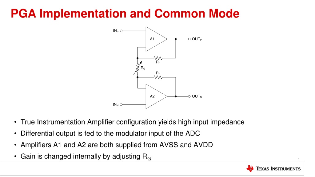
PGA Implementation and Common Mode INP A1 OUTP RF RG RF A2 OUTN INN True Instrumentation Amplifier configuration yields high input impedance Differential output is fed to the modulator input of the ADC Amplifiers A1 and A2 are both supplied from AVSS and AVDD Gain is changed internally by adjusting RG 1
Defining a Common Language INP A1 OUTP RF VCM = (VINP + VINN)/2 VIN RG VOUT = Gain VIN RF A2 OUTN INN Differential Input Voltage: PGA Gain: Differential Output Voltage: Input/Output Common-Mode Voltage: VIN Gain= 1 + 2 RF/RG VOUT= (VOUTP VOUTN) = Gain VIN VCM= (VINP+ VINN) / 2 = (VOUTP+ VOUTN) / 2 = (VINP VINN) (*) All absolute voltages are referenced to AVSS 2
Common-mode Voltage Limitation INP A1 OUTP VIN VOUT RF RG RF VOUT = Gain VIN VIN A2 OUTN INN (*)Use the largest input signal that can occur in your application for VIN A1 and A2 are not rail-to-rail output amplifiers. In ADS1248 e.g. they can only drive ~0.1V to the rails. Therefore OUTP and OUTN have to be > (AVSS + 0.1V) or < (AVDD - 0.1V) at all times for the amplifiers to stay in their linear operating regions. VOUTN = VCM Gain VIN AVSS + 0.1V ! Gain V Gain V + + AVSS 0 1 . V V AVDD 0 1 . V IN IN CM 2 2 3
Example II: Gain = 1 INP 1.1V 1.1V A1 OUTP 1.1V VCM = 0.6V 1V 1V RG 0.1V A2 OUTN 0.1V INN 0.1V Requirement: Gain V IN = + + V AVSS 0 . 1 V CM MIN 2 1 1 V = + + = V 0 V 0 . 1 V 0 . 6 V CM MIN 2 4
Common-mode Voltage Violation, Gain = 1 INP 1V 1V A1 OUTP 1V 1V VCM = 0.5V 1V RG 0V A2 OUTN 0V !!! INN 0V Requirement: Gain V IN = + + V AVSS 0 . 1 V CM MIN 2 1 1 V = + + = V 0 V 0 . 1 V 0 . 6 V CM MIN 2 5