High Voltage and Front-end Electronics for iRPC Upgrade
Detailed information regarding the high voltage configurations and front-end electronics setups for the upgraded Resistive Plate Chambers (RPCs). It covers different RPC designs, operational voltages, chamber configurations, HV connections, and power consumption data for the front-end electronics. The content also includes images and technical specifications discussed during the RPC upgrade meetings.

Download Presentation

Please find below an Image/Link to download the presentation.
The content on the website is provided AS IS for your information and personal use only. It may not be sold, licensed, or shared on other websites without obtaining consent from the author. Download presentation by click this link. If you encounter any issues during the download, it is possible that the publisher has removed the file from their server.
E N D
Presentation Transcript
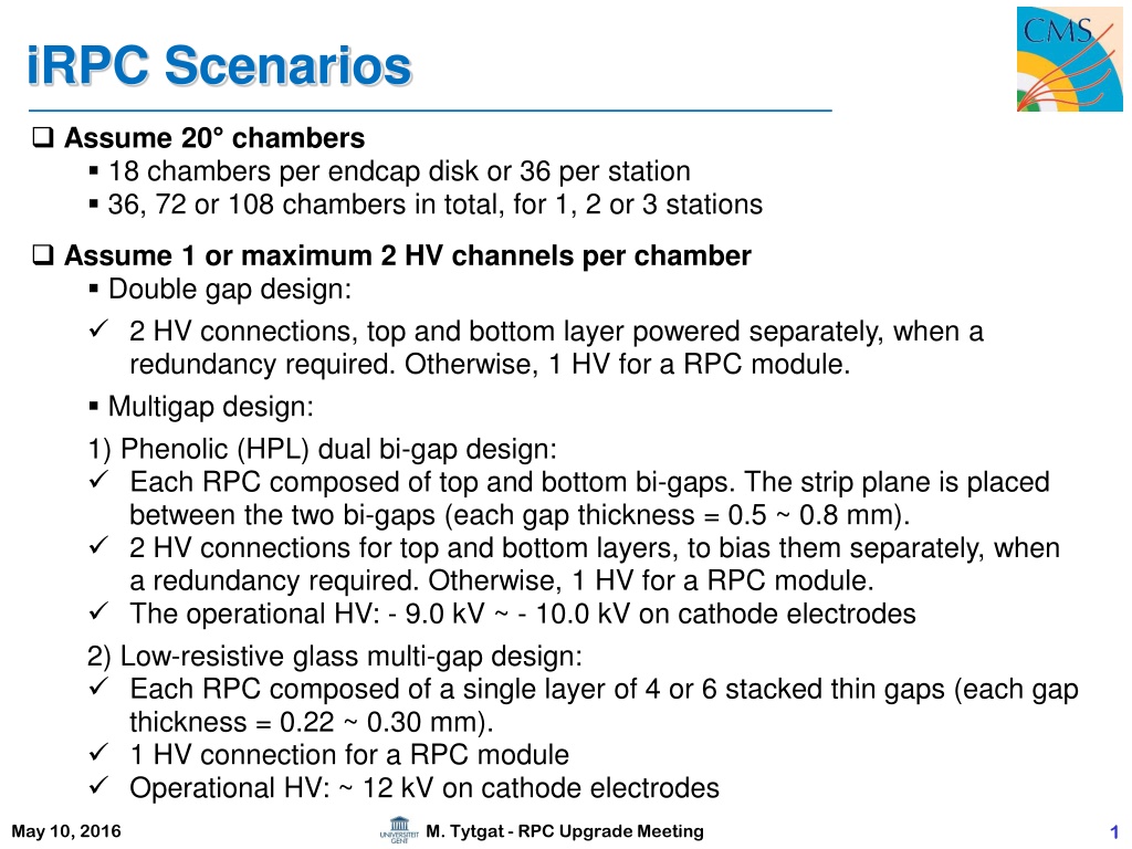
iRPC Scenarios Assume 20 chambers 18 chambers per endcap disk or 36 per station 36, 72 or 108 chambers in total, for 1, 2 or 3 stations Assume 1 or maximum 2 HV channels per chamber Double gap design: 2 HV connections, top and bottom layer powered separately, when a redundancy required. Otherwise, 1 HV for a RPC module. Multigap design: 1) Phenolic (HPL) dual bi-gap design: Each RPC composed of top and bottom bi-gaps. The strip plane is placed between the two bi-gaps (each gap thickness = 0.5 ~ 0.8 mm). 2 HV connections for top and bottom layers, to bias them separately, when a redundancy required. Otherwise, 1 HV for a RPC module. The operational HV: - 9.0 kV ~ - 10.0 kV on cathode electrodes 2) Low-resistive glass multi-gap design: Each RPC composed of a single layer of 4 or 6 stacked thin gaps (each gap thickness = 0.22 ~ 0.30 mm). 1 HV connection for a RPC module Operational HV: ~ 12 kV on cathode electrodes May 10, 2016 M. Tytgat - RPC Upgrade Meeting 1
Standard double-gap RPC Low-resistive glass multi-gap RPC Phenolic dual bi-gap RPC M. Tytgat - RPC Upgrade Meeting 2 May 10, 2016
Front-end Electronics Present FEB electronics (32 ch) 2 LV channels per chamber (or per 2 chambers?) Assume present granularity, i.e. 64 strips/20 ; 5 partitions per chamber, i.e. 5x2 FEBs or 320 ch/chamber 2.6W/FEB, i.e. 26W/chamber PETIROC electronics (64ch in new version?) Assume 2mm pitch, i.e. ~565 strips/20 ;1 -partition (both end strip readout), i.e. 9 ASICs/chamber 3mW/ch (?), i.e. 1.7W/chamber (ASICs only, what about TDC?) M. Tytgat - RPC Upgrade Meeting 3 May 10, 2016
iRPC Scenarios: wrap-up I Assume 20 chambers 18 chambers per endcap disk or 36 per station RE3/1 36 chambers RE4/1 36 chambers Assume 1 or maximum 2 HV channels per chamber Double gap design: top and bottom layer powered separately? MG Lyon (glass): 1 HV connection per chamber (300 m x 4 || 5 layers), negative polarity from 0 to - 12/13 kV. Remark: EASY HV boards A3512N used presently at CMS can power up to 12kV max. MG Korea (HPL): 1 HV cable per chamber, WP ~ 9KV (neg. polarity) Front-end Electronics Present FEB electronics (32 channels) 2 LV channels (ANA && DIG) per 2 chambers, powered by 12-channel A3009 board, 8V, 45W max. Assume present granularity, i.e. 64 strips/20 ; 5 partitions per chamber, i.e. 5x2=10 FEBs or 320 channels/chamber Power Consumption/Currents (A) LV_ANA 0.029A per chip, 0.116A per FEB, 1.16A per chamber LV_DIG 0.066A per chip, 0.264A per FEB, 2.64A per chamber Power Consumption/Dissipation (W) LV_ANA 0.203W per chip, 0.812W per FEB, 8.12W per chamber LV_DIG 0.495W per chip, 1.98W per FEB, 19.8W per chamber 2.792W per FEB, i.e. ~28W per chamber Remark: see next page May 11, 2016 2
iRPC Scenarios: little evolution Present FEB electronics (continue from previous page) Remark: Using present CAEN LV power boards A3009, they provide 45W max per channel, divided by 8V (the max Voltage we can provide per this type of module), it makes 5.625A the max. value of current to be drawn by all FEBs. Divided by the DIG current drawn by a single FEB, it finally makes that 21 FEBs can be powered by one A3009 channel, which means that we can still preserve the present powering schema (2 LV channels powering 2 chambers). However, this value is very close to the power failure limit of the board and we risk to experience a lot of HVmax errors while powering. Therefore, I will prepare the following alternative powering schemas: 2 A3009 LV channels powering one 20 chamber; 2 A3016 LV channels powering two 20 chambers. In this option the powering schema is the same as the present CMS detector, but we use a different type of board where the max power per channel is 90W, but the number of channel per board are 6 instead of 12. This option will increase the number of boards and the cost. However, we will be using about 50% of the power, so it is possible another solution, namely 2 A3016 LV channels powering three 20 chambers. In this case 75% of the power of the board will be used which is quite optimal regime of operation and it is also cost saving. 2 A3009 LV channels powering two 20 chambers. This is the present CMS RPC LV powering scheme which I discourage to use as explained above. May 11, 2016 Wrap-up 2
iRPC Scenarios: wrap-up II Developing FEB electronics PETIROC electronics (64ch in new version) on ASIC TDC Assume ~3mm pitch, i.e. 320 strips per 20 or 640 channels (320 strips readout on both ends);1 -partition i.e. 10 ASICs x 64 channels each = 640 channels. Power consumption: 3.6 mW per channel x 640 = 2.3W per 20 chamber Question: How are these channels powered? How many volts, how many PCB, how is the LV power distributed? on FPGA TDC Assume ~3mm pitch, i.e. 320 strips/20 or 640 channels. Power consumption: ~80mW per channel x 640 = 51W per chamber Strip Readout? In general, for the cabling I would need more details on how those strips will be read out. At present, a front-end LVDS driver is converting the signal to LVDS which is sent to the Link boards (LB) located in the periphery towers where the signal is multiplexed and converted to optical by an optical driver. Then the fibers go from the towers to the PP at the bottom of each tower and from the PP they go through the tunnel to reach the Trigger Boards (TB) in USC. This chain is not quite clear to me at present for the new electronics. Can anyone elaborate on this? From the last meeting I only wrote down the following: 1 OF per chamber going to GBT board DAQ, but what these GBT boards are and how they would be integrated into existing CMS electronics (CMS compatibility) where will they be located? This is extremely important to evaluate the length of the optical fibers, we need the endpoints (obviously one end is the chamber, but where is the other length?) May 11, 2016 2