Understanding Sputtering Systems for Thin Film Deposition
Sputtering systems, including DC and RF sputtering, are used for thin film deposition of metals, dielectrics, and alloys. This process involves ejecting atoms from a solid target material through bombardment by energetic particles. The efficiency of sputtering is measured by sputter yield, which depends on various factors like energy of incident ions and mass of target atoms. Different sputtering technologies like magnetron and reactive sputtering offer versatile options for various deposition requirements.

Download Presentation

Please find below an Image/Link to download the presentation.
The content on the website is provided AS IS for your information and personal use only. It may not be sold, licensed, or shared on other websites without obtaining consent from the author. Download presentation by click this link. If you encounter any issues during the download, it is possible that the publisher has removed the file from their server.
E N D
Presentation Transcript
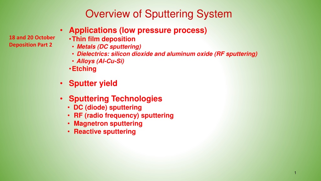
Overview of Sputtering System Applications (low pressure process) Thin film deposition Metals (DC sputtering) Dielectrics: silicon dioxide and aluminum oxide (RF sputtering) Alloys (Al-Cu-Si) Etching 18 and 20 October Deposition Part 2 Sputter yield Sputtering Technologies DC (diode) sputtering RF (radio frequency) sputtering Magnetron sputtering Reactive sputtering 1
Basic Sputtering System DC or RF 2
Mechanisms of Sputtering Sputtering is a process that atoms are ejected from a solid target material due to bombardment of the target by energetic particles Reflected ions and neutral atoms Incident ions Secondary electrons + Sputtered ions from the target material Surface Target material Ions with very low energy may be reflected away from the surface. Ions with energy less than 10eV, could also be adsorbed to the surface, giving up their energy as heat. Ions with energy above about 5keV, will penetrate into the material and transfer their energy to atoms in the target material. Ions with medium energy, transfer part of energy to heat and use the other part of energy for physical rearrangement of the target surface. The atoms of the target materials will be ejected out. 4
Sputter Yield Sputtering process is characterized by sputter yield (S), which is a measure of efficiency of sputtering ejected atoms or moledules = S incident ions Sputter yield depends on: the energy of incident ions the mass of incident ions the mass of target atoms the binding energy of atoms in the target the incident angle of ions M ln 1 E gas S cos M E target 5
Sputter Yield (Contd) For each target material, there exists a threshold energy, below which no sputtering occurs 6
DC and RF Sputtering System DC sputtering: Used for sputtering metal materials, such as Al, Ti, and Au. The target acts as the cathode in a diode system RF sputtering: Used for dielectric materials, such as SiO2, and Al2O3. (Using DC sputtering for dielectric material will cause the buildup of positive charges on the target. The alternating potential voltage can avoid the charge buildup) DC or RF 7
Pressure Effect Optimal pressure is around 100mTorr (1Torr =133Pa) Compromise between increasing number of Ar ions increasing scattering of Ar ions with neutral Ar atoms How to increase the number of Ar ions without increasing the pressure? Magnetron sputtering 8
CVD-Various Techniques Atmospheric pressure CVD (APCVD) CVD at atmospheric pressure Low-pressure CVD (LPCVD) CVD at sub-atmospheric pressures Ultrahigh vacuum CVD (UHVCVD) CVD at very low pressure, typically below 10 6 Pa (~10 8 torr)
Polysilicon Polycrystalline silicon is deposited from trichlorosilane (SiHCl3) or silane (SiH4), using the following reactions:[ SiH3Cl Si + H2 + HCl SiH4 Si + 2 H2 Silicon Dioxide SiH4 + O2 SiO2 + 2 H2 SiCl2H2 + 2 N2O SiO2 + 2 N2 + 2 HCl Si(OC2H5)4 SiO2 + byproducts Silicon Nitride Silicon nitride is often used as an insulator and chemical barrier in manufacturing ICs. The following two reactions deposit silicon nitride from the gas phase: 3 SiH4 + 4 NH3 Si3N4 + 12 H2 3 SiCl2H2 + 4 NH3 Si3N4 + 6 HCl + 6 H2 Or to deposit SiNH: 2 SiH4 + N2 2 SiNH + 3 H2 SiH4 + NH3 SiNH + 3 H2 Metals WF6 W + 3 F2 WF6 + 3 H2 W + 6 HF Similar reactions for Al using triisobutylaluminium (TIBAL) [Organometallic compounds] Molybdenum, Tantalum, Titanium-Recall we discussed silicides earlier this semester.
A process that uses ions of an inert gas to dislodge atoms from the surface of a crystalline material, the atoms then being electrically deposited to form an extremely thin coating on a glass, metal, plastic, or other surface.
Designs of Magnetron Sputtering System SM: solenoid magnet M: magnet E: electric field B: Magnetic field T: Target P: Plasma S: Substrate Advantages: Could be used together with DC or RF Higher sputter efficiency due to the increase of ionization of Ar atoms Higher sputter rate under lower pressure (10-5 or 10-3 Torr) Increase probability of electrons striking Ar atoms 14
Parameters for Magnetron Sputtering Deposition pressure : 10 Deposition pressure : 10- -5 5 to 10 Pressure for DC or RF Sputtering: Pressure for DC or RF Sputtering: ~ ~ 0.1 Pressure for evaporation: Pressure for evaporation: ~ ~ 0.01 to 10- -3 3 Torr Torr 0.1 Torr Torr Torr 0.01 Torr Deposition rate : 0.2 ~ 2 Deposition rate : 0.2 ~ 2 m/min 10 times higher than DC or RF sputtering 10 times higher than DC or RF sputtering Deposition rate for evaporation is 2 ~5 Deposition rate for evaporation is 2 ~5 m/min m/min m/min Deposition temperature: 100 to 150 Deposition temperature: 100 to 150o oC C Evaporation temperature is above 1000oC 15
Reactive Sputtering Sputtering metallic target in the presence of a reactive gas mixed with inert gas (Ar) A mixture of inert +reactive gases used for sputtering oxides Al2O3, SiO2, Ta2O5 (O2) nitrides TaN, TiN, Si3N4 (N2, NH3) carbides TiC, WC, SiC (CH4, C2H4, C3H8) Chemical reaction takes place on substrate and target Can poison target if chemical reactions are faster than sputter rate Adjust reactive gas flow to get good stoichiometry without incorporating excess gas into film 16
Comparison between Evaporation and Sputtering Evaporation Sputtering Low energy atoms (~ 0.1 eV) High energy atoms/ions (10 20 eV) Better adhesion Higher pressure for DC/RF, but much lower pressure for magnetron sputtering Poor directional Argon atoms implanted in the film Better step coverage Low pressure, high vacuum Directional in nature Lower impurity Poor step coverage Point source, poor uniformity Parallel plate source, better uniformity For compound materials and alloys, different components evaporate at different rate, which leads to poor stoichiometry For compound materials, all components sputtered with similar rate, which helps maintain stoichiometry Physical process DC, RF, and magnetron sputtering are physical processes Reactive sputtering is chemical process 17
Chemical vapor deposition (CVD) Physics and Chemistry in CVD process Atmospheric CVD (APCVD) Low pressure CVD (LPCVD) Plasma-enhanced CVD (PECVD) Metal organic CVD (MOCVD) 19
Simple CVD Reactor Temperature of the susceptor should be maintained, which is more challenging for PECVD system. Cooling system inside the susceptor in PECVD: plasma discharge increased the susceptor temperature. Cooling is performed by circulating a coolant through a tube inside the susceptor in order to sustain the susceptor temperature for large-area and high rate deposition. (YB Lim, et al., Int. J. Precis. Eng. Man., 13(7), 2012) 20
Physics and Chemistry in the Reactor CVD Process: Introduce reactive gases to the chamber Thermal decomposition of the gases through heat or plasma Gas absorption by substrate surface Reaction takes place on substrate surface and film is firmed Transport of volatile byproducts away form substrate Exhaust waste Example: SiH4 (g) Si (s) +2H2 (g) (for polysilicon) Physics and chemistry involved: (1) Dilution of the SiH4 The decomposition of silane gas (SiH4) around the susceptor decreased the deposition rate and concentration of silane along the length of the reactor; The silane can be mixed with in an inert carrier gas, i.e., H2, to improve the uniformity of deposition; The surface will have concentration of vacancies brought by H2. (2) Homogeneous and Heterogeneous reaction Homogeneous: atoms of the solid are released from the gas (undesired) Heterogeneous: atoms of the solid form on the wafer surface (preferred) 21
Physics and Chemistry in the Reactor (2) Example: SiH4 (g) Si (s) +2H2 (g) (3) Other reactions in the reactor SiH4(g) SiH2 (s) +H2 (g) SiH4 (g)+ SiH2(g) Si2H6 (g) SiH6(g) HSi2H3(g)+H2(g) How to judge which reaction is dominant? The equilibrium constant for each reaction. (4) Gas flow: Gas flow determines the transport of the various chemical species in the chamber Important for temperature distribution (5) Temperature effects: Deposition rate Uniformity Hot wall batch CVD reactor: for large batch processes, excellent temperature control, but low deposition rate 22
Atmospheric CVD (APCVD) Features: High reaction rate, poor uniformity and purity Run at atmospheric pressure Used for thick dielectrics with deposition rate higher than 1000 /min Example: SiH4 (g) + O2(g) SiO2 (s) +2H2 (g) 23
Low Pressure CVD (LPCVD) Features: Hot wall system and cold wall systems: Hot wall system: uniform temperature distributions, but has deposition on the walls Cold wall system: with reduced deposition on the walls Used for polysilicon and dielectrics (mostly in hot wall systems) Good purity, low deposition rate than APCVD Low pressure in the chamber (0.1 to 1.0 Torr) Temperature 550 ~ 650 C 24
Plasma Enhanced CVD (PECVD) Features: Deposit at low substrate temperature Used to deposit dielectrics over Al or GaAs Use plasma to enhance the decomposition and reaction in the CVD Very good at filling small features May induce plasma damage Plasma may increase the substrate temperature, so cooling on the substrate is important Temperature can be as low as 120 C 25
Metal Organic CVD (MOCVD) Features Use gaseous organic precursors Advantages: highly flexible > can deposit semiconductors, metals, dielectrics Disadvantages: highly toxic, very expensive source material, environmental disposal costs are high. Uses: dominates low cost optical (but not electronic) III-V technology, some metallization 26
Summary on CVD APCVD LPCVD PECVD MOCVD Advantages High growth rate at atmospheric pressure Low pressure, Low temperature flexible high purity Good for filling small features Disadvantage Poor purity Low growing rate Plasma damage Toxic, expensive source materials Materials Thick dielectric materials Poly-Si and dielectric materials Dielectrics over Al or GaAs III-V materials 27
Epitaxy What is it: deposition of a crystalline overlayer on a crystalline substrate. Requirement: the substrate must act as seed crystal with preferred crystal orientation Application: to deposit single-crystal silicon (30~100 m), compound semiconductors and semiconductor heterojunctions Epitaxy methods: Vapor phase epitaxy (VPE) (very common) Molecular beam epitaxy (MBE) Process: Wafer cleaning: to remove native oxide and any residual impurities and particles RCA cleaning procedure: (1) remove organic residues (SC-1); (2) remove thin oxide layer; (3) remove metallic contaminations (SI-2) Epitaxy growth 28
Molecular Beam Epitaxy (MBE) MBE process: The crystalline layer is formed by deposition from a thermal beam of atoms or molecules. Deposition is performed in ultrahigh vacuum conditions (10-10 Torr) Substrate temperature: 400 ~900 C Application: Growth thickness with atomic resolution Good growth quality for semicondutor heterostructures 29
Vapor Phase Epitaxy (VPE) Process A simple VPE system. VPE steps: (1) Gas phase decomposition; (2) Transport to the surface of the wafer; At the surface: (3) Adsorb; (4) Diffuse; (5) Decompose (6) By-product desorb 30


")


")


")
")
")
")
")


")
 Process")
 Process")
 Process")
 Process")
 Process")
 Process")