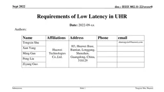
Understanding Latency in JESD204B Links
Latency in a JESD204B link refers to the time it takes for a signal to travel from input to output, influenced by factors like system setup, device dependencies, clock propagation delays, and signal alignment. Definitions such as Sample-to-Serial Out (S2SO), Link Delay, and Link Latency are crucial in describing different aspects of latency within the JESD204B framework. Understanding and managing latency is essential for optimizing data transfer efficiency in advanced communication systems.

Download Presentation

Please find below an Image/Link to download the presentation.
The content on the website is provided AS IS for your information and personal use only. It may not be sold, licensed, or shared on other websites without obtaining consent from the author. Download presentation by click this link. If you encounter any issues during the download, it is possible that the publisher has removed the file from their server.
E N D
Presentation Transcript
What is Latency? Latency is defined as the total time (in seconds or clock cycles) it takes a signal to travel from Point A to Point B In a system: Point A might be the input to the ADC Point B might be the output of the DAC In a JESD204B link: Point A is the input to the JESD204B transmitter Point B is the output of the JESD204B receiver s elastic buffer
JESD204B Latency Influencers Device dependent SYSREF propagation delay JESD link layer Serdes implementation Board level Channel (trace length, vias, connectors) SYSREF propagation delay Clock propagation delay
JESD204B System Diagram (Subclass 1) Data is sent over serdes lanes Each device receives a SYSREF signal to align LMFCs in each device Each device receives a device clock which is essentially the sample clock The device clock captures the SYSREF signal so setup and hold times must be met
Latency Definitions Sample-to-Serial Out (S2SO) Latency S2SO is the latency from when the signal is sampled at the ADC input until the sample appears in the serial stream at the ADC (TX) output.
Latency Definitions Link Delay Link delay is the delay from when the sampled parallel data is input to the serializer at the transmitter (ADC) until the same data is presented at the input to the elastic buffer.
Latency Definitions Link Latency Link latency is the latency from when the sampled parallel data is input to the serializer at the transmitter (ADC) until the same data is available in parallel form at the receiver.
Latency Definitions Sample-to-Parallel Out (S2PO) Latency S2PO is the latency from when the signal is sampled at the ADC input until the sample is released on the parallel bus at the receiving device (RX).
What is Deterministic Latency? Wikipedia: A deterministic system is a system in which no randomness is involved in the development of future states of the system. A deterministic model will thus always produce the same output from a given starting condition or initial state. The most important aspect of deterministic latency is that the latency should stay constant from system startup to startup. Having deterministic latency does not necessarily mean the latency is known How do we achieve deterministic latency? JESD204B defines two mechanisms for deterministic latency called subclasses
JESD204B Subclasses Subclass Subclass 0 Mechanism for Deterministic Latency No support for deterministic latency (backward compatible with JESD204A). SYSREF signal is used to align LMFCs within all TX and RX devices. SYNC signal is used to align LMFCs, eliminating the need for SYSREF . LMFC is aligned based on when the SYNC signal is received from each data converter device. Complex timing means that this will only work below 500 MSPS. Subclass 1 Subclass 2
What Systems May Need Deterministic Latency? Applications sensitive to latency Digital pre-distortion (DPD) control loops Automatic gain control loops (AGC) Defensive counter measures Any system that requires multi-device synchronization Multi antenna transmit/receive Phased array radar Magnetic Resonance Imaging (MRI)
How Does JESD204B Achieve Deterministic Latency? Sequence of events for subclass 1: 1. SYSREF is sent to all devices at the same point in time to align their local multi-frame clocks 2. All transmitters issue an /A/ character at the same point in time based on the LMFC clock edge. - Channel and device variations will skew the lanes relative to each other 3. As each RX receives the /A/ character, it starts to buffer it s data 4. Once all RXs receive their /A/ character and the buffer release point has been reached (e.g. LMFC rising edge), all RXs release their data from the buffer which is now time aligned
Initial Lane Alignment Sequence TX transmits ILA starting at an LMFC edge ILA is 4 multi-frames, containing configuration parameters and alignment symbols (A) used for multiframe alignment The /A/ or /R/ characters are the key for deterministic latency
Deterministic Latency Visual 1. SYSREF is used to align LMFCs received, all lanes send ILAS on next LMFC edge when it receives the trigger (R or A char) 4. All lanes are released on the 2. After SYNC is 3. Each lane starts buffering it s data next LMFC edge and are now aligned x
How is Deterministic Latency Guaranteed?
How Do We Guarantee Deterministic Latency? 1. Guarantee the LMFCs in each device are aligned (or have constant phase difference) every time the system starts 2. Set release point to occur after the latest arriving lane by: Having total link delay less than the LMFC period Setting a buffer release point that occurs after all lanes have arrived This is what the standard expects, but it s not always possible!
1. Aligning the LMFCs in Each Device The LMFCs need to be aligned in each device to create a known timing reference point All devices should receive SYSREF at the same time every time the system starts SYSREF must meet setup and hold times relative to device clocks Technically the LMFCs can be misaligned, but the phase difference needs to be the same every time the system starts
2. Set Release Point to Occur After the Latest Arriving Lane The LMFC period is decided by the linerate, F (octets per frame), and K (frames per multi-frame) LMFC period = 10 * F * K / Linerate 10 = number of bits per octet For example, if F = 8, K = 16, and the linerate is 7372.8 Mbps, then the LMFC period is 173.6 ns. In the example, the total link delay should be less than 173.6 ns
How do we set the release point? Why is there variation on the data delay? Consider the following scenario: The LMFC period is 50 ns The delay for each lane is 100 ns +/- 10 ns (90 ns to 110 ns) Assume the buffer release point is set to the LMFC clock rising edge
Release Point The latest arriving lane arrives at 90 ns 50 ns Data delay is 90 ns Total latency is 100 ns
Release Point The latest arriving lane arrives at 110 ns 50 ns Data delay is 110 ns Total latency is 150 ns
Incorrect Release Point In this example, the latency IS NOT deterministic because it is not consistent from startup to startup How do we avoid this scenario? 1. Calculate the expected maximum lane delay 2. Choose a release point that occurs after the maximum lane delay
Release Point occurs RBD frame cycles after the LMFC boundary Set RBD = K/2 Using RBD to shift the release point 50 ns RBD Data delay is 110 ns Total latency is 125 ns
The Three Step Process 1. Determine Alignment of LMFCs 2. Calculate expected link delay (accounting for variation) 3. Choose release point that provides margin against error 4. Calculate total latency by adding ADC or DAC latency
Step 1: Determine Alignment of LMFCs Things to consider: Propagation delay of SYSREF and device clocks across board Purposefully added delays to SYSREF, such as analog delays or dynamic digital delays (see LMK04828) Delays from SYSREF input pins to resetting of LMFC (internal to devices)
LMFC Alignment Between Devices LMFC is not always reset as soon as SYSREF is captured. The SYSREF pin to LMFC reset timing may be different for each device. Some datasheets will specify SYSREF to LMFC timing for various modes (e.g. DAC38J84) and this delay needs to be added to the LMFC delay.
Variations occur due to device variances (specified in datasheet) or due to PVT effects Step 2: Calculate Link Delay These delays will come from the datasheet or need to be measured or calculated Total Link Delay = tTX_SER + tLANE + tRX_DESER +/- tVARIANCE LMFC alignment between TX and RX has already been determined
Choose release point that guarantees enough margin around the expected lane arrival Step 3: Choose Buffer Release Point
Summary of Calculation We have done the following: 1. Determined LMFC alignment between TX and RX 2. Calculated total link delay 3. Determined the appropriate buffer release point 3 2 1
Total Link Latency The total link latency can be calculated using the following formula Link Latency = (n * K + RBD) * TFRAME + (tRX_LMFC tTX_LMFC) Where n is the number of whole RX multi-frames traversed n = 2 1 2
How is Deterministic Latency Verified?
Test Setup 1. Generate a pulse with FPGA 2. Capture pulse with ADC 3. Output ADC s MSB from FPGA 4. Observed relative timing on scope 5. Power up the system many times to confirm the relative timing stays constant
Device Setup ADC = ADC16DX370 (16-bit, dual channel, 370 MSPS) Device clock = 370 MHz (2.7 ns) JESD204B Parameters L = 4, M = 2, F = 1, S = 1, K = 32 Frame cycle = 10 * F / Linerate = 10 * 1 / 3700 Mbps = 2.7 ns LMFC cycle = Frame cycle * K = 2.7 ns * 32 = 86.4 ns FPGA Device clock = 92.5 MHz (10.8 ns)
Additional Delays in System O-Scope 12in. Coax 1.6ns Ch.A Input Pulse Splitter 12in. Coax 1.6ns 3in. Rogers4350 0.5ns 18in. Coax 2.3ns ADC FPGA Ch.B 2in. Rogers4350 0.3ns Total Added Latency (due to routing) = (1.6+0.5+2.3)- (1.6)+(1.3-0.3) = 3.8ns LMK 8in. Rogers4350 1.3ns
Latency Calculation Per the previous slides, the latency is calculated as Link Latency = (n * K + RBD) * TFRAME + (tRX_LMFC tTX_LMFC) For this experiment the following parameters apply All units in Frame clock cycles tRX_LMFC = 28, tTX_LMFC = 3.5, n = 2, K = 32, RBD=28 (RX_BUFFER_DELAY=4) Link Latency = 116.5 frame clock cycles The following also extend the latency ADC16DX370 core latency = +12.5 DEVCLK routing skew and MSB output routing delay = +1.4 SYSREF/DEVCLK sampling skew = +1.5 Additional receiver processing delays +3 rx_tdata release delay (for earliest sample in the 4-sample set output each period of 92.5MHz clock. This delay may instead be +4) +4 latching MSBs before output (at Fs/4 rate) Total Calculated Latency = 116.5 + 12.5 + 1.4 + 1.5 + 7 = 138.9 cycles
Result Latency=379.6ns Calculated latency for this setup is 138.9 frame cycles Measured latency is 379.6 ns / 2.7 ns = 140.4 cycles Note: Would have been better to use a short pulse as test signal to avoid confusion over correct output pulse
Whats the easiest way to achieve deterministic latency? Setup a test similar to the one shown to observe relative delays Vary RBD until a 1 LMFC period jump is observed, then add the expected latency variation to that value (plus extra margin) Release Release Release Release Release Release Point Point Point Point Point Point Total Latency Optimal Release Point


")